Contents
Introduction
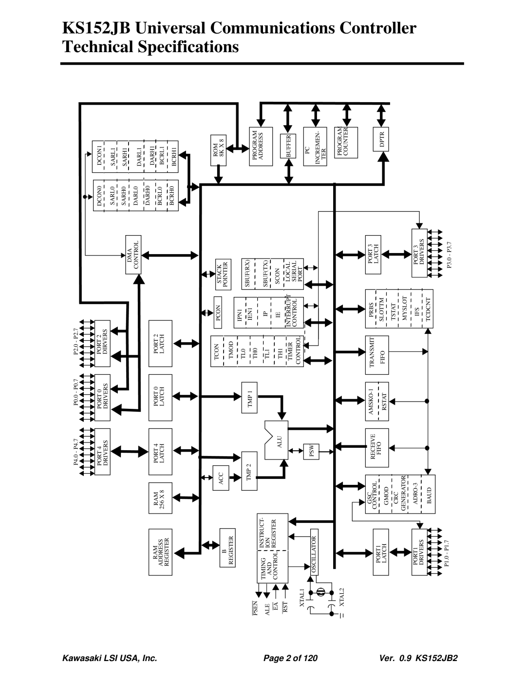
Technical Specifications
Name Description Port
Pin Description
PIN Description
Pin Name Alternate Function
RST
XTAL1
XTAL2
Eben
ALE
Psen
Epsen
Special function Registers
SFR map for the cpu
Reset Timing Reset Values of the SFRs
Sbuf Indeterminate Tmod
Configurations
Scon
Pcon
Port 0 I/O Pad Port 2 I/O Pad
Port bit I/O Pads
Ports 4,5
Comments
Program
Psen Epsen
Fetch via
TIMER/COUNTERS
Tmod Timer/Counter Mode Control Register
Tcon Timer/Counter Control Register
Mode
Timer/Counter in Mode
Interrupts
Timer/Counter 0 in Mode
IE Interrupt Enable Register
Priority Level Structure
Egste EDMA1 Egstv EDMA0 Egsre Egsrv
Pgste PDMA1 Pgstv PDMA0 Pgsre Pgsrv
Pgsrv
PX0
EX0
Egsrv 2BH
PT1
PDMA1
EDMA1
ET1 1BH
Kawasaki LSI USA, Inc Ver .9 KS152JB2
ALE Psen
Power Down and Idle
Status of the External Pins during Idle and Power Down
Pcon Power Control Register
Smod IDL
Local Serial Channel
Local Serial Port Mode
Controller
Serial Port Mode
Mode
Load Sbuf
Baud Rates
MHZ
Timer 1 generated commonly used Baud rates
Smod
Reti
SINGLE-STEP Operation
JNB
Kawasaki LSI USA Inc
Global Serial Channel
Introduction
11/IDLE CRC None
DC JAM CRC
Csma Sdlc
11/IDLE
External clock Internal clock
Control cpu Control dma Raw Receive Raw Transmit
Preamble BOF Address Info CRC EOF
CSMA/CD Overview
CSMA/CD Frame Format
Kawasaki LSI USA, Inc Ver .9 KS152JB2
23 24
Interframe Space
Collision Detection
CSMA/CD Data Encoding
Manchester Encoding BIT Time
Jitter Tolerance
Unexpected 1-to-0 Transition
Narrow Pulses
Missing 0-to-1 Transition
Response to a Detected Collision What the GSC was doing
Resolution of Collisions
GSC Inactive
Tfifo
Algorithm
Backoff
DCR
BKOFF= Myslot
Random Backoff
Prbs Tcdcnt Load Bkoff Slot Clock Myslot
Deterministic Backoff
Hardware Based Acknowledge
Kawasaki LSI USA, Inc Ver .9 KS152JB2
Sdlc Frame Format
BOF Address Control Info CRC EOF
Kawasaki LSI USA, Inc Ver .9 KS152JB2
BIT STUFFING/STRIPPING
Data Encoding
Nrzi BIT Time
Acknowledgement
Sending Abort Character
Line Idle
Multi-Drop Network
PRIMARY/SECONDARY Stations
Point-to-point Network
Ring Network
Sdlc Hdlc
Using a Preamble in Sdlc
HDLC/SDLC Comparison
User Defined Protocols
Line Discipline
Planning for Network Changes and Expansions
DMA Servicing of GSC Channels
Kawasaki LSI USA, Inc Ver .9 KS152JB2
Baud Rate
Initialization
Test Modes
External Driver Interface
Jitter Receive
BIT Time Received
Local Value Manchester Encoding BIT Time
Receive Sampling Rate Received
Transmit Waveforms
Receiver Clock Recovery
CSMA/CD Clock Recovery
Rcbat Crce
Determining Receiver Errors
External Clocking
Addressing
Determining Line Discipline
2 CPU/DMA Control of the GSC
Collisions and Backoff
What the GSC was doing Response
GSC Register Descriptions
Successful Ending of Transmissions and Receptions
GMOD84H Xtclk PL1 PL0
PL1 PL0 Length Bits
Kawasaki LSI USA, Inc Ver .9 KS152JB2
DCJ DCR SA5 SA4 SA3 SA2 SA1 SA0
ARB REQ Garen Xrclk Gfien IDL
Rcabt Crce RDN Rfne Gren Haben
Kawasaki LSI USA, Inc Ver .9 KS152JB2
LNI Noack Tcdt TDN Tfnf TEN DMA
Kawasaki LSI USA, Inc Ver .9 KS152JB2
DMA Operation
DMA with the 80C152
DMA Registers
DAS IDA
Alternate Cycle Mode
Burst Mode
SAS ISA
Serial Port Demand Mode
External Demand Mode
PCH P2 SFR DMA Cycle Resume Program Execution
Timing Diagrams
12 OSC.PERIODS ALE Psen P1 Inst Float
DMA Transfer from Internal Memory to Internal Memory
DMA Cycle Resume Program Execution
12 OSC. Periods ALE Psen Inst DMA Data OUT PCL Inst PCH
DMA Cycle 12 OSC. Periods Resume Program Execution ALE Psen
Hold/Hold Acknowledge
Request Mode
Arbiter Mode
Using the HOLD/HLDA Acknowledge
ARB REQ
Dmxrq
ALE ARB If Hlda = ALE AEQ ALE REQ
Internal Logic of the Arbiter
Internal Logic of the Requester
DMA Arbitration
Kawasaki LSI USA, Inc.oup, Inc Ver .9 KS152JB2
Kawasaki LSI USA, Inc Ver .9 KS152JB2
Kawasaki LSI USA, Inc Ver .9 KS152JB2
DMA Arbitration with Hold/Hold Ack
Summary of DMA Control Bits
DAS IDA SAS ISA Done
Interrupt Structure
IE0
TI+RI
ET1 EX1 ET0 EX0
PT1 PX1 PT0 PX0
IPN1
GSC Transmitter Error Conditions
Transmit Error Flags Logic for Clearing TEN, Setting TDN
GSC Receiver Error Conditions
Glossary
Kawasaki LSI USA, Inc Ver .9 KS152JB2
DCON0/1 092H,093H
Xtclk PL1 PL0
Kawasaki LSI USA, Inc 102 Ver .9 KS152JB2
Kawasaki LSI USA, Inc 103 Ver .9 KS152JB2
PT1 PX1 PT0 EX0
Myslot 0F5H DCJ DCR SA5 SA4 SA3 SA2 SA1 SA0
Smod ARB REQ Garen Xrclk Gfien IDL
OVR Rcabt Crce RDN Rfne Gren Haben
Kawasaki LSI USA, Inc 108 Ver .9 KS152JB2
SM0 SM1 SM2 REN TB8 RB8
TF1 TR1 TF0 TR0 IE1 IT1 IE0 IT0
Gate
Kawasaki LSI USA, Inc 111 Ver .9 KS152JB2
Data Pointer LOW
Port
Stack Pointer
DPL.7 DPL.6 DPL5 DPL.4 DPL.3 DPL.2 DPL.1 DPL.0
DPH.7 DPH.6 DPH.5 DPH.4 DPH.3 DPH.2 DPH.1 DPH.0
Timer Control
Data Pointer High
DPH
Timer 0 LSB
Timer Mode Control
Gate Timer
Timer 1 LSB
Timer 0 MSB
Timer 1 MSB
Serial Data Buffer
Serial Port Control
SM0
SBUF.7
Program Status Word
RS1 RS0
Accumulator
ACC.7 ACC.6 ACC.5 ACC.4 ACC.3 ACC.2 ACC.1 ACC.0
Kawasaki LSI USA, Inc 119 Ver .9 KS152JB2
Kawasaki LSI USA, Inc 120 Ver .9 KS152JB2

