KS152JB Universal Communications Controller Technical Specifications
2.2 Special function Registers
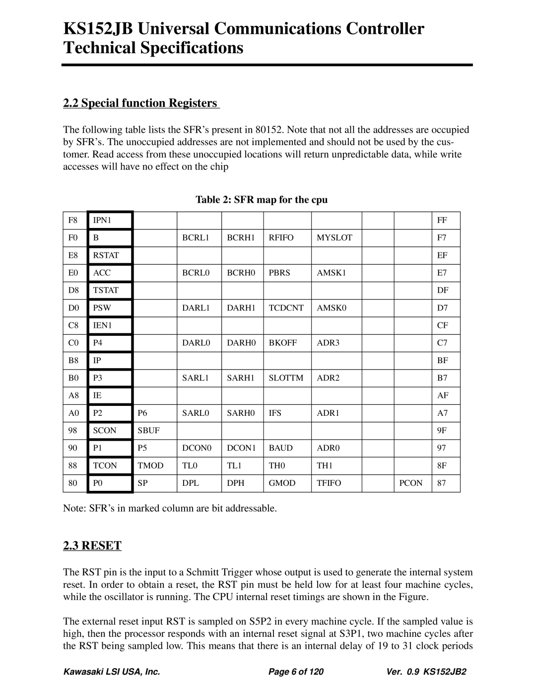
The following table lists the SFR’s present in 80152. Note that not all the addresses are occupied by SFR’s. The unoccupied addresses are not implemented and should not be used by the cus- tomer. Read access from these unoccupied locations will return unpredictable data, while write accesses will have no effect on the chip
Table 2: SFR map for the cpu
F8 | IPN1 |
|
|
|
|
|
|
| FF |
|
|
|
|
|
|
|
|
|
|
F0 | B |
| BCRL1 | BCRH1 | RFIFO | MYSLOT |
|
| F7 |
|
|
|
|
|
|
|
|
|
|
E8 | RSTAT |
|
|
|
|
|
|
| EF |
|
|
|
|
|
|
|
|
|
|
E0 | ACC |
| BCRL0 | BCRH0 | PBRS | AMSK1 |
|
| E7 |
|
|
|
|
|
|
|
|
|
|
D8 | TSTAT |
|
|
|
|
|
|
| DF |
|
|
|
|
|
|
|
|
|
|
D0 | PSW |
| DARL1 | DARH1 | TCDCNT | AMSK0 |
|
| D7 |
|
|
|
|
|
|
|
|
|
|
C8 | IEN1 |
|
|
|
|
|
|
| CF |
|
|
|
|
|
|
|
|
|
|
C0 | P4 |
| DARL0 | DARH0 | BKOFF | ADR3 |
|
| C7 |
|
|
|
|
|
|
|
|
|
|
B8 | IP |
|
|
|
|
|
|
| BF |
|
|
|
|
|
|
|
|
|
|
B0 | P3 |
| SARL1 | SARH1 | SLOTTM | ADR2 |
|
| B7 |
|
|
|
|
|
|
|
|
|
|
A8 | IE |
|
|
|
|
|
|
| AF |
|
|
|
|
|
|
|
|
|
|
A0 | P2 | P6 | SARL0 | SARH0 | IFS | ADR1 |
|
| A7 |
|
|
|
|
|
|
|
|
|
|
98 | SCON | SBUF |
|
|
|
|
|
| 9F |
|
|
|
|
|
|
|
|
|
|
90 | P1 | P5 | DCON0 | DCON1 | BAUD | ADR0 |
|
| 97 |
|
|
|
|
|
|
|
|
|
|
88 | TCON | TMOD | TL0 | TL1 | TH0 | TH1 |
|
| 8F |
|
|
|
|
|
|
|
|
|
|
80 | P0 | SP | DPL | DPH | GMOD | TFIFO |
| PCON | 87 |
|
|
|
|
|
|
|
|
|
|
Note: SFR’s in marked column are bit addressable.
2.3 RESET
The RST pin is the input to a Schmitt Trigger whose output is used to generate the internal system reset. In order to obtain a reset, the RST pin must be held low for at least four machine cycles, while the oscillator is running. The CPU internal reset timings are shown in the Figure.
The external reset input RST is sampled on S5P2 in every machine cycle. If the sampled value is high, then the processor responds with an internal reset signal at S3P1, two machine cycles after the RST being sampled low. This means that there is an internal delay of 19 to 31 clock periods
Kawasaki LSI USA, Inc. | Page 6 of 120 | Ver. 0.9 KS152JB2 |