KS152JB Universal Communications Controller Technical Specifications
can be masked in AMSK1:AMSK0. A received address of all ones will always be recognized in any mode. The user software is responsible for setting or clearing this flag.
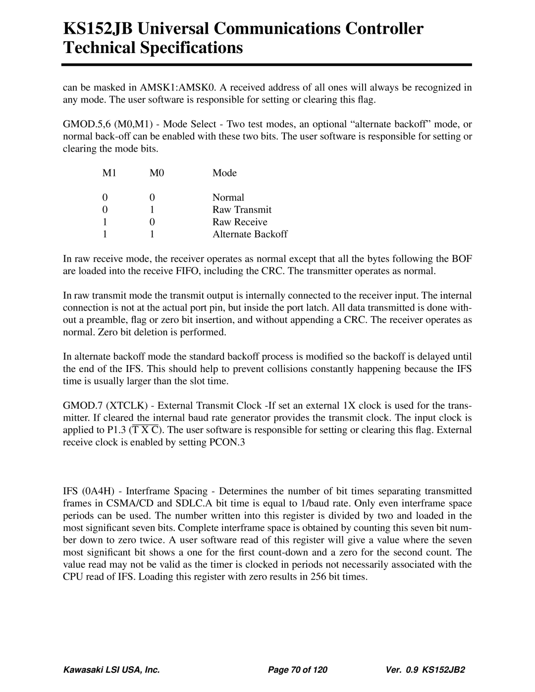
GMOD.5,6 (M0,M1) - Mode Select - Two test modes, an optional “alternate backoff” mode, or normal
M1 | M0 | Mode |
0 | 0 | Normal |
0 | 1 | Raw Transmit |
1 | 0 | Raw Receive |
1 | 1 | Alternate Backoff |
In raw receive mode, the receiver operates as normal except that all the bytes following the BOF are loaded into the receive FIFO, including the CRC. The transmitter operates as normal.
In raw transmit mode the transmit output is internally connected to the receiver input. The internal connection is not at the actual port pin, but inside the port latch. All data transmitted is done with- out a preamble, flag or zero bit insertion, and without appending a CRC. The receiver operates as normal. Zero bit deletion is performed.
In alternate backoff mode the standard backoff process is modified so the backoff is delayed until the end of the IFS. This should help to prevent collisions constantly happening because the IFS time is usually larger than the slot time.
GMOD.7 (XTCLK) - External Transmit Clock
IFS (0A4H) - Interframe Spacing - Determines the number of bit times separating transmitted frames in CSMA/CD and SDLC.A bit time is equal to 1/baud rate. Only even interframe space periods can be used. The number written into this register is divided by two and loaded in the most significant seven bits. Complete interframe space is obtained by counting this seven bit num- ber down to zero twice. A user software read of this register will give a value where the seven most significant bit shows a one for the first
Kawasaki LSI USA, Inc. | Page 70 of 120 | Ver. 0.9 KS152JB2 |