KS152JB Universal Communications Controller Technical Specifications
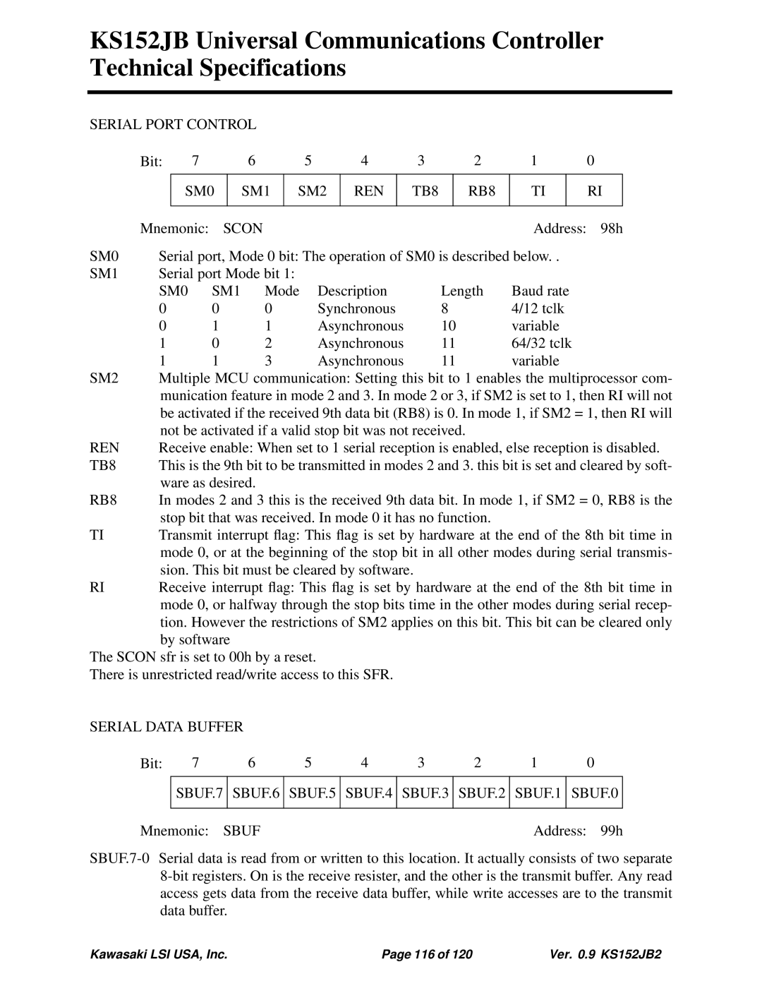
SERIAL PORT CONTROL |
|
|
|
|
|
|
|
|
|
|
| ||||||
| Bit: | 7 | 6 |
| 5 |
| 4 |
| 3 | 2 | 1 |
| 0 |
| |||
|
|
|
|
|
|
|
|
|
|
|
|
|
|
|
| ||
|
| SM0 |
| SM1 |
| SM2 | REN |
| TB8 |
| RB8 | TI |
| RI |
| ||
|
|
|
|
|
|
|
|
|
|
|
|
|
|
|
|
| |
| Mnemonic: | SCON |
|
|
|
|
|
|
| Address: | 98h | ||||||
SM0 | Serial port, Mode 0 bit: The operation of SM0 is described below. . |
|
| ||||||||||||||
SM1 | Serial port Mode bit 1: |
|
|
|
|
|
|
|
|
|
|
| |||||
| SM0 | SM1 Mode | Description |
| Length | Baud rate |
|
| |||||||||
| 0 |
| 0 | 0 |
|
| Synchronous |
| 8 |
| 4/12 tclk |
|
| ||||
| 0 |
| 1 | 1 |
|
| Asynchronous |
| 10 | variable |
|
| |||||
| 1 |
| 0 | 2 |
|
| Asynchronous |
| 11 | 64/32 tclk |
|
| |||||
| 1 |
| 1 | 3 |
|
| Asynchronous |
| 11 | variable |
|
| |||||
SM2 | Multiple MCU communication: Setting this bit to 1 enables the multiprocessor com- | ||||||||||||||||
| munication feature in mode 2 and 3. In mode 2 or 3, if SM2 is set to 1, then RI will not | ||||||||||||||||
| be activated if the received 9th data bit (RB8) is 0. In mode 1, if SM2 = 1, then RI will | ||||||||||||||||
| not be activated if a valid stop bit was not received. |
|
|
|
| ||||||||||||
REN | Receive enable: When set to 1 serial reception is enabled, else reception is disabled. | ||||||||||||||||
TB8 | This is the 9th bit to be transmitted in modes 2 and 3. this bit is set and cleared by soft- | ||||||||||||||||
| ware as desired. |
|
|
|
|
|
|
|
|
|
|
| |||||
RB8 | In modes 2 and 3 this is the received 9th data bit. In mode 1, if SM2 = 0, RB8 is the | ||||||||||||||||
| stop bit that was received. In mode 0 it has no function. |
|
|
|
| ||||||||||||
TI | Transmit interrupt flag: This flag is set by hardware at the end of the 8th bit time in | ||||||||||||||||
| mode 0, or at the beginning of the stop bit in all other modes during serial transmis- | ||||||||||||||||
| sion. This bit must be cleared by software. |
|
|
|
|
|
| ||||||||||
RI | Receive interrupt flag: This flag is set by hardware at the end of the 8th bit time in | ||||||||||||||||
| mode 0, or halfway through the stop bits time in the other modes during serial recep- | ||||||||||||||||
| tion. However the restrictions of SM2 applies on this bit. This bit can be cleared only | ||||||||||||||||
| by software |
|
|
|
|
|
|
|
|
|
|
| |||||
The SCON sfr is set to 00h by a reset. |
|
|
|
|
|
|
|
|
|
| |||||||
There is unrestricted read/write access to this SFR. |
|
|
|
|
|
|
| ||||||||||
SERIAL DATA BUFFER |
|
|
|
|
|
|
|
|
|
|
| ||||||
| Bit: | 7 | 6 |
| 5 |
| 4 |
| 3 | 2 | 1 |
| 0 |
| |||
|
|
| |||||||||||||||
|
| SBUF.7 | SBUF.6 | SBUF.5 | SBUF.4 | SBUF.3 | SBUF.2 | SBUF.1 | SBUF.0 |
| |||||||
|
|
|
|
|
|
|
|
|
|
|
|
|
|
|
|
| |
| Mnemonic: | SBUF |
|
|
|
|
|
|
| Address: | 99h | ||||||
Kawasaki LSI USA, Inc. | Page 116 of 120 | Ver. 0.9 KS152JB2 |