KS152JB Universal Communications Controller Technical Specifications
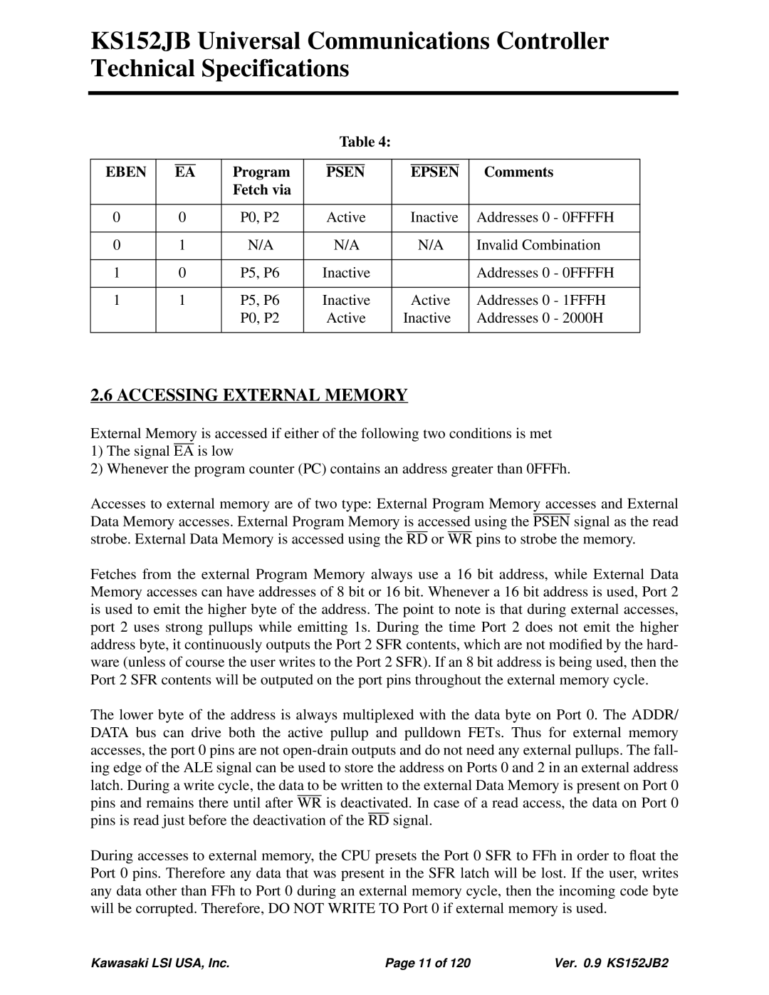
Table 4:
|
|
|
|
|
|
|
|
|
|
|
|
|
EBEN |
| EA | Program |
| PSEN |
| EPSEN | Comments | ||||
|
|
|
| Fetch via |
|
|
|
|
|
|
|
|
|
|
|
|
|
|
|
|
|
|
|
|
|
0 | 0 |
| P0, P2 | Active | Inactive | Addresses 0 | - 0FFFFH | |||||
|
|
|
|
|
|
|
|
|
|
|
| |
0 | 1 |
| N/A |
| N/A |
| N/A | Invalid Combination | ||||
|
|
|
|
|
|
|
|
|
|
|
|
|
1 | 0 |
| P5, P6 | Inactive |
|
|
| Addresses 0 | - 0FFFFH | |||
|
|
|
|
|
|
|
|
|
|
|
|
|
1 | 1 |
| P5, P6 | Inactive |
| Active | Addresses 0 | - 1FFFH | ||||
|
|
|
| P0, P2 |
| Active | Inactive | Addresses 0 | - 2000H | |||
|
|
|
|
|
|
|
|
|
|
|
|
|
2.6 ACCESSING EXTERNAL MEMORY
External Memory is accessed if either of the following two conditions is met
1)The signal EA is low
2)Whenever the program counter (PC) contains an address greater than 0FFFh.
Accesses to external memory are of two type: External Program Memory accesses and External Data Memory accesses. External Program Memory is accessed using the PSEN signal as the read strobe. External Data Memory is accessed using the RD or WR pins to strobe the memory.
Fetches from the external Program Memory always use a 16 bit address, while External Data Memory accesses can have addresses of 8 bit or 16 bit. Whenever a 16 bit address is used, Port 2 is used to emit the higher byte of the address. The point to note is that during external accesses, port 2 uses strong pullups while emitting 1s. During the time Port 2 does not emit the higher address byte, it continuously outputs the Port 2 SFR contents, which are not modified by the hard- ware (unless of course the user writes to the Port 2 SFR). If an 8 bit address is being used, then the Port 2 SFR contents will be outputed on the port pins throughout the external memory cycle.
The lower byte of the address is always multiplexed with the data byte on Port 0. The ADDR/ DATA bus can drive both the active pullup and pulldown FETs. Thus for external memory accesses, the port 0 pins are not
During accesses to external memory, the CPU presets the Port 0 SFR to FFh in order to float the Port 0 pins. Therefore any data that was present in the SFR latch will be lost. If the user, writes any data other than FFh to Port 0 during an external memory cycle, then the incoming code byte will be corrupted. Therefore, DO NOT WRITE TO Port 0 if external memory is used.
Kawasaki LSI USA, Inc. | Page 11 of 120 | Ver. 0.9 KS152JB2 |
