KS152JB Universal Communications Controller Technical Specifications
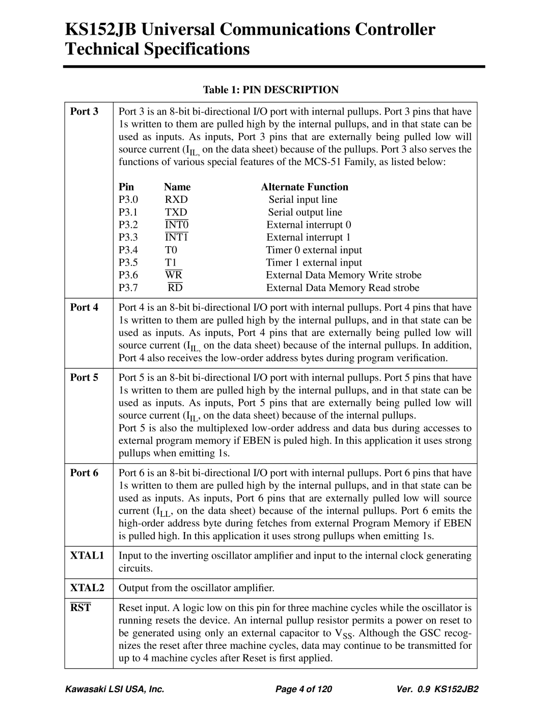
| Table 1: PIN DESCRIPTION |
|
|
Port 3 | Port 3 is an |
| 1s written to them are pulled high by the internal pullups, and in that state can be |
| used as inputs. As inputs, Port 3 pins that are externally being pulled low will |
| source current (IIL, on the data sheet) because of the pullups. Port 3 also serves the |
| functions of various special features of the |
|
|
| Pin | Name | Alternate Function | |||||
|
|
| P3.0 |
| RXD | Serial input line | ||||
|
|
| P3.1 |
| TXD | Serial output line | ||||
|
|
| P3.2 |
|
|
|
|
|
| External interrupt 0 |
|
|
|
| INT0 | ||||||
|
|
| P3.3 |
|
|
|
|
|
| External interrupt 1 |
|
|
|
| INT1 | ||||||
|
|
| P3.4 |
| T0 | Timer 0 external input | ||||
|
|
| P3.5 |
| T1 | Timer 1 external input | ||||
|
|
| P3.6 |
|
|
|
|
| External Data Memory Write strobe | |
|
|
|
| WR | ||||||
|
|
| P3.7 |
|
|
|
| External Data Memory Read strobe | ||
|
|
|
|
| RD | |||||
|
|
| ||||||||
| Port 4 | Port 4 is an | ||||||||
|
|
| 1s written to them are pulled high by the internal pullups, and in that state can be | |||||||
|
|
| used as inputs. As inputs, Port 4 pins that are externally being pulled low will | |||||||
|
|
| source current (IIL, on the data sheet) because of the internal pullups. In addition, | |||||||
|
|
| Port 4 also receives the | |||||||
|
|
| ||||||||
| Port 5 | Port 5 is an | ||||||||
|
|
| 1s written to them are pulled high by the internal pullups, and in that state can be | |||||||
|
|
| used as inputs. As inputs, Port 5 pins that are externally being pulled low will | |||||||
|
|
| source current (IIL, on the data sheet) because of the internal pullups. | |||||||
|
|
| Port 5 is also the multiplexed | |||||||
|
|
| external program memory if EBEN is puled high. In this application it uses strong | |||||||
|
|
| pullups when emitting 1s. |
| ||||||
|
|
| ||||||||
| Port 6 | Port 6 is an | ||||||||
|
|
| 1s written to them are pulled high by the internal pullups, and in that state can be | |||||||
|
|
| used as inputs. As inputs, Port 6 pins that are externally pulled low will source | |||||||
|
|
| current (ILL, on the data sheet) because of the internal pullups. Port 6 emits the | |||||||
|
|
| ||||||||
|
|
| is pulled high. In this application it uses strong pullups when emitting 1s. | |||||||
|
|
| ||||||||
| XTAL1 | Input to the inverting oscillator amplifier and input to the internal clock generating | ||||||||
|
|
| circuits. |
|
|
|
|
|
|
|
|
|
| ||||||||
| XTAL2 | Output from the oscillator amplifier. | ||||||||
|
|
|
| |||||||
|
|
| Reset input. A logic low on this pin for three machine cycles while the oscillator is | |||||||
| RST | |||||||||
|
|
| running resets the device. An internal pullup resistor permits a power on reset to | |||||||
|
|
| be generated using only an external capacitor to VSS. Although the GSC recog- | |||||||
|
|
| nizes the reset after three machine cycles, data may continue to be transmitted for | |||||||
|
|
| up to 4 machine cycles after Reset is first applied. | |||||||
Kawasaki LSI USA, Inc. | Page 4 of 120 | Ver. 0.9 KS152JB2 |