KS152JB Universal Communications Controller Technical Specifications
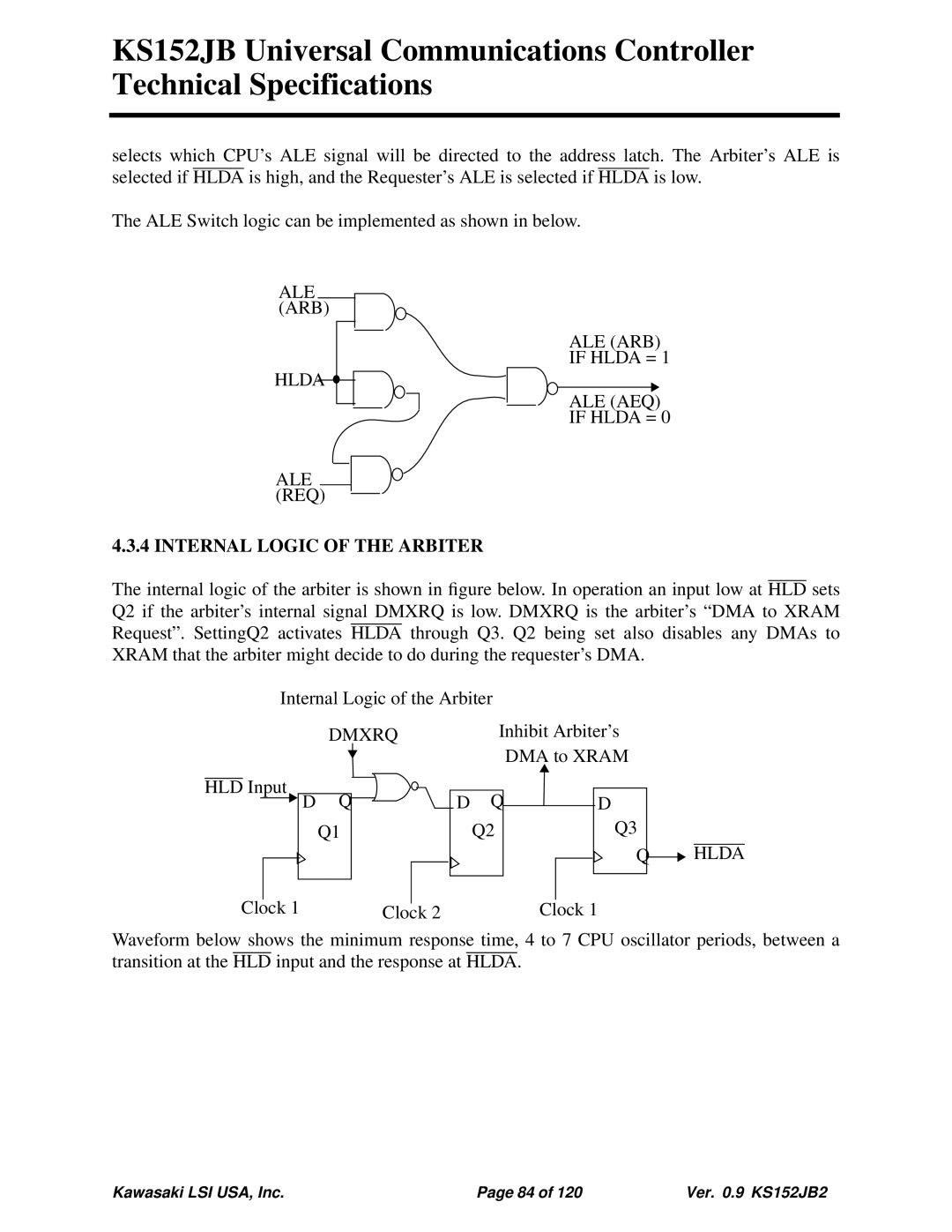
selects which CPU’s ALE signal will be directed to the address latch. The Arbiter’s ALE is selected if HLDA is high, and the Requester’s ALE is selected if HLDA is low.
The ALE Switch logic can be implemented as shown in below.
ALE (ARB)
ALE (ARB)
IF HLDA = 1
HLDA ![]()
ALE (AEQ)
IF HLDA = 0
ALE (REQ)
4.3.4 INTERNAL LOGIC OF THE ARBITER
The internal logic of the arbiter is shown in figure below. In operation an input low at HLD sets Q2 if the arbiter’s internal signal DMXRQ is low. DMXRQ is the arbiter’s “DMA to XRAM Request”. SettingQ2 activates HLDA through Q3. Q2 being set also disables any DMAs to XRAM that the arbiter might decide to do during the requester’s DMA.
Internal Logic of the Arbiter
DMXRQ
HLD Input
![]() D Q
D Q![]()
Q1
Inhibit Arbiter’s DMA to XRAM
D Q ![]() D
D
Q2Q3
Q ![]() HLDA
HLDA
Clock 1 | Clock 2 | Clock 1 |
Waveform below shows the minimum response time, 4 to 7 CPU oscillator periods, between a transition at the HLD input and the response at HLDA.
Kawasaki LSI USA, Inc. | Page 84 of 120 | Ver. 0.9 KS152JB2 |
