Section TOC
Master TOC
TROUBLESHOOTING & REPAIR
CONTROL PC BOARD TEST (continued)
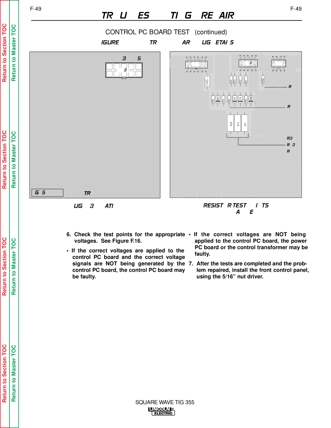
FIGURE F.16 – CONTROL PC BOARD PLUG DETAILS
Return to
Return to Section TOC
Return to
Return to Master TOC
1 2 3 4 5
J13
10 9 8 7 6
CONTROL |
PLUG J13 LOCATION
J12 |
| J13 |
| J14 |
|
|
| • | R66 |
|
|
|
| |
• |
|
|
| R8 |
• | • | • |
| R32 |
|
|
|
| |
|
|
|
| R13 |
|
|
|
| R11 |
RESISTOR TEST POINTS
(Control Board Area Enlarged)
Return to Section TOC
Return to Master TOC
6.Check the test points for the appropriate voltages. See Figure F.16.
•If the correct voltages are applied to the control PC board and the correct voltage signals are NOT being generated by the control PC board, the control PC board may be faulty.
•If the correct voltages are NOT being applied to the control PC board, the power PC board or the control transformer may be faulty.
7.After the tests are completed and the prob- lem repaired, install the front control panel, using the 5/16” nut driver.
Return to Section TOC
Return to Master TOC
SQUARE WAVE TIG 355