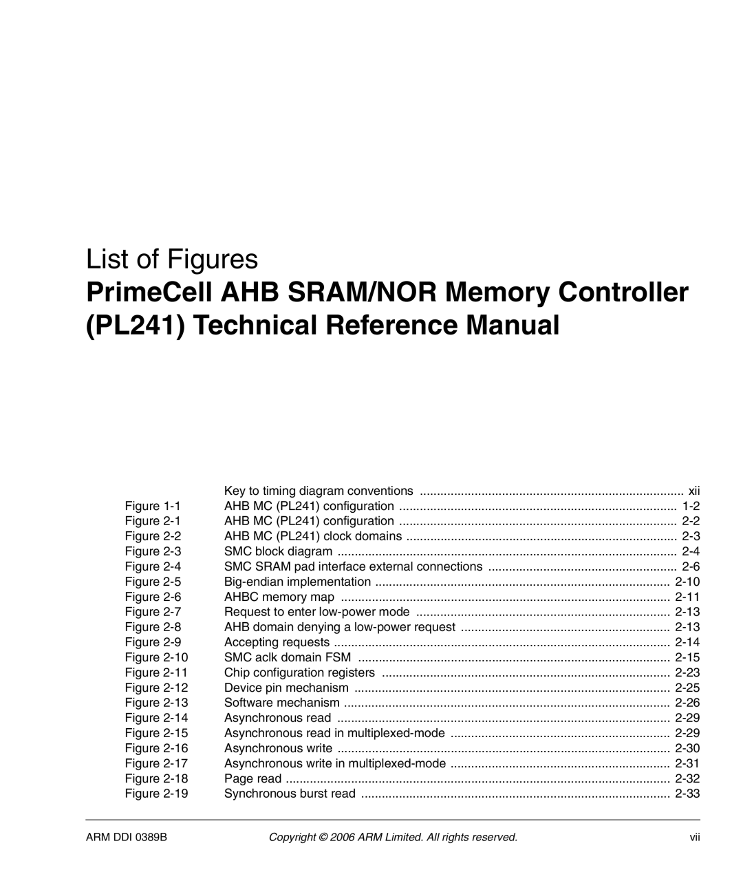
List of Figures
PrimeCell AHB SRAM/NOR Memory Controller (PL241) Technical Reference Manual
| Key to timing diagram conventions | xii |
Figure | AHB MC (PL241) configuration | |
Figure | AHB MC (PL241) configuration | |
Figure | AHB MC (PL241) clock domains | |
Figure | SMC block diagram | |
Figure | SMC SRAM pad interface external connections | |
Figure | ||
Figure | AHBC memory map | |
Figure | Request to enter | |
Figure | AHB domain denying a | |
Figure | Accepting requests | |
Figure | SMC aclk domain FSM | |
Figure | Chip configuration registers | |
Figure | Device pin mechanism | |
Figure | Software mechanism | |
Figure | Asynchronous read | |
Figure | Asynchronous read in | |
Figure | Asynchronous write | |
Figure | Asynchronous write in | |
Figure | Page read | |
Figure | Synchronous burst read |
ARM DDI 0389B | Copyright © 2006 ARM Limited. All rights reserved. | vii |
