Functional Overview
Read data output by the memory device is also registered on the rising edge of
smc_mclk0n, equivalent to the falling edge of smc_mclk0, for asynchronous reads. For synchronous reads, read data is registered using the fed back clock, smc_fbclk_in. For synchronous and asynchronous accesses, the data is then pushed onto the read data FIFO to be returned by the SMC interface.
This subsection describes:
•Asynchronous read
•Asynchronous read in
•Asynchronous write on page
•Asynchronous write in
•Asynchronous page mode read on page
•Synchronous burst read on page
•Synchronous burst read in
•Synchronous burst write on page
•Synchronous burst write in
•Synchronous read and asynchronous write on page
Asynchronous read
Table
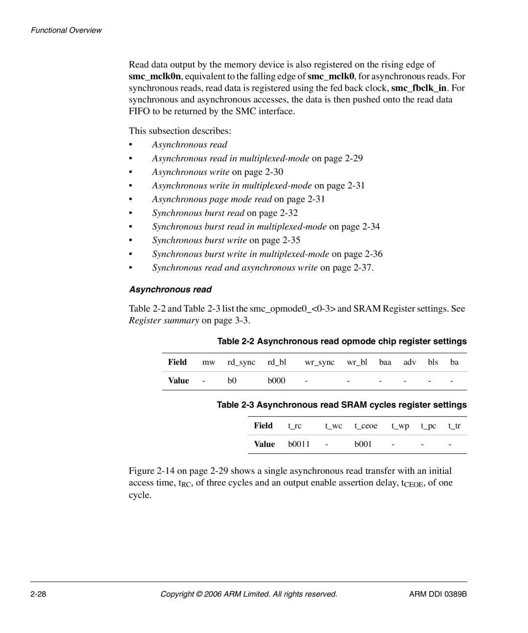
Table 2-2 Asynchronous read opmode chip register settings
Field | mw | rd_sync rd_bl | wr_sync | wr_bl | baa | adv | bls | ba | ||
|
|
|
|
|
|
|
|
|
|
|
Value | - | b0 | b000 | - |
| - | - | - | - | - |
|
|
| ||||||||
|
| Table | ||||||||
|
|
|
|
|
|
|
|
|
|
|
|
|
| Field | t_rc | t_wc | t_ceoe |
| t_wp | t_pc | t_tr |
|
|
|
|
|
|
|
|
|
|
|
|
|
| Value | b0011 | - | b001 |
| - | - | - |
|
|
|
|
|
|
|
|
|
|
|
Figure 2-14 on page 2-29 shows a single asynchronous read transfer with an initial access time, tRC, of three cycles and an output enable assertion delay, tCEOE, of one cycle.
Copyright © 2006 ARM Limited. All rights reserved. | ARM DDI 0389B |