Functional Overview
Synchronous read and asynchronous write
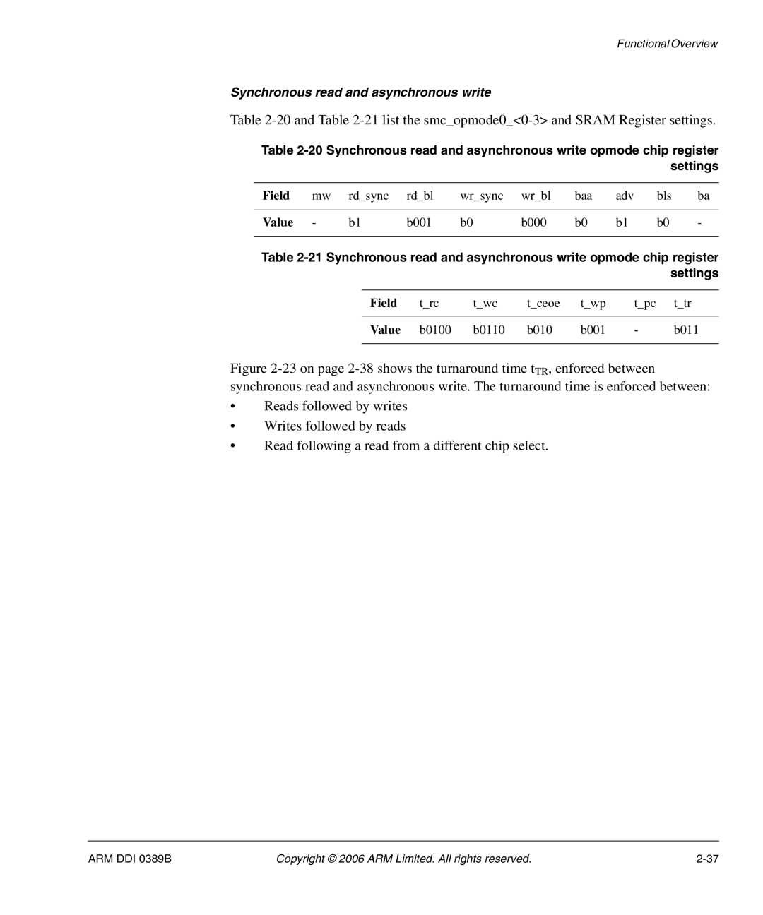
Table 2-20 and Table 2-21 list the smc_opmode0_<0-3> and SRAM Register settings.
Table
Field | mw | rd_sync | rd_bl | wr_sync | wr_bl | baa | adv | bls | ba |
|
|
|
|
|
|
|
|
|
|
Value | - | b1 | b001 | b0 | b000 | b0 | b1 | b0 | - |
|
|
|
|
|
|
|
|
|
|
Table
Field | t_rc | t_wc | t_ceoe | t_wp | t_pc | t_tr |
|
|
|
|
|
|
|
Value | b0100 | b0110 | b010 | b001 | - | b011 |
|
|
|
|
|
|
|
Figure 2-23 on page 2-38 shows the turnaround time tTR, enforced between synchronous read and asynchronous write. The turnaround time is enforced between:
•Reads followed by writes
•Writes followed by reads
•Read following a read from a different chip select.
ARM DDI 0389B | Copyright © 2006 ARM Limited. All rights reserved. |