a | MicroConverter®, Multichannel | |
|
|
|
|
| ADuC812 |
|
|
|
FEATURES
ANALOG I/O
DMA Controller for
MEMORY
8K Bytes
640Bytes
256Bytes
16M Bytes External Data Address Space
64K Bytes External Program Address Space
8051-COMPATIBLE CORE
12 MHz Nominal Operation (16 MHz Max) Three
High Current Drive
Nine Interrupt Sources, Two Priority Levels
POWER
Specified for 3 V and 5 V Operation Normal, Idle, and
Power Supply Monitor
APPLICATIONS
Intelligent Sensors Calibration and Conditioning
Battery Powered Systems (Portable PCs, Instruments,
Monitors)
Transient Capture Systems
DAS and Communications Systems
Control Loop Monitors (Optical Networks/Base Stations)
GENERAL DESCRIPTION
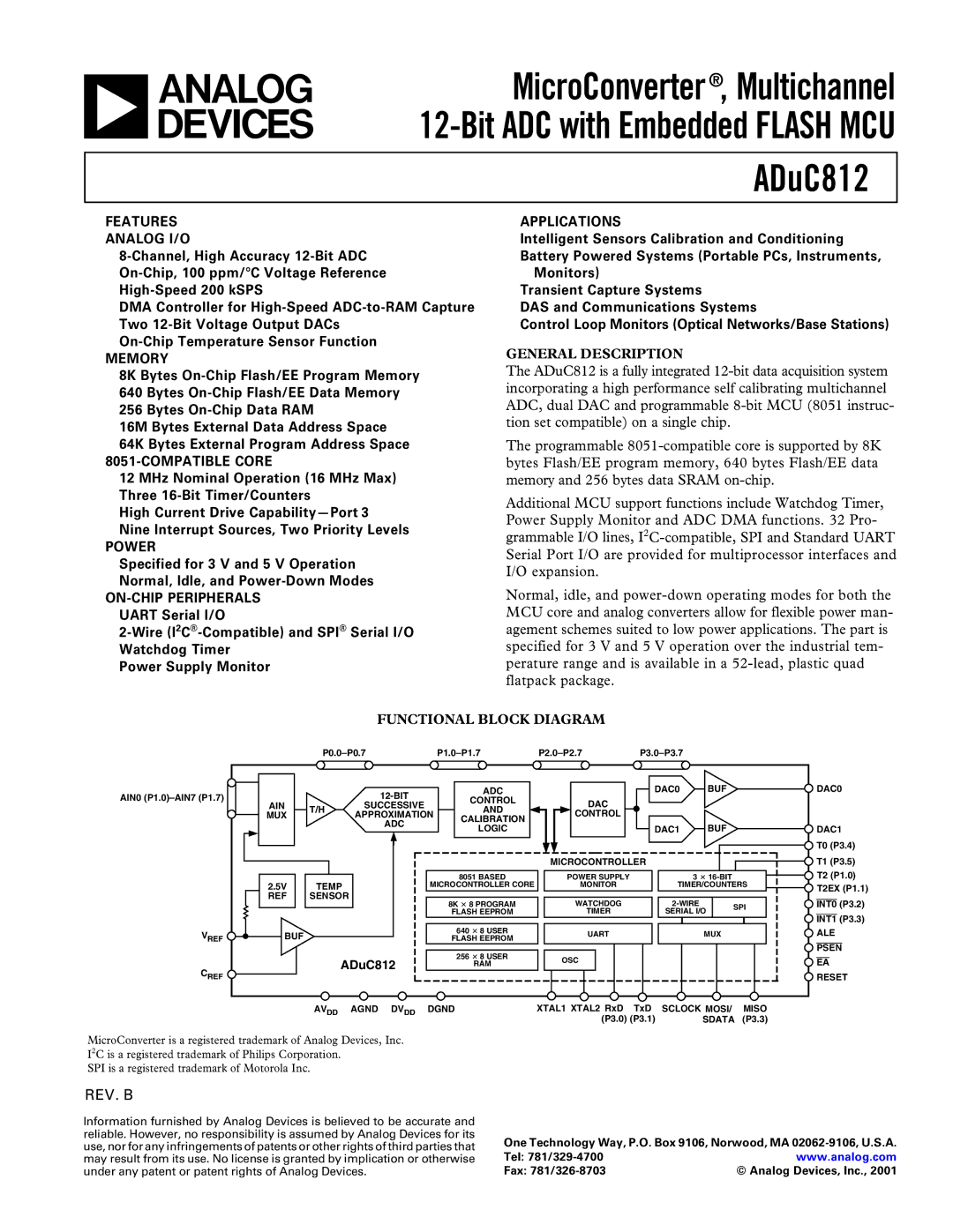
The ADuC812 is a fully integrated
The programmable
Additional MCU support functions include Watchdog Timer, Power Supply Monitor and ADC DMA functions. 32 Pro- grammable I/O lines,
Normal, idle, and
FUNCTIONAL BLOCK DIAGRAM
|
|
|
|
|
|
| ||||||||
AIN0 |
|
|
|
|
| ADC |
|
| DAC0 | BUF |
|
| DAC0 | |
|
|
|
|
| CONTROL | DAC |
|
|
|
|
|
| ||
| AIN | T/H | SUCCESSIVE |
|
|
|
|
|
|
|
| |||
|
|
| AND |
|
|
|
|
|
| |||||
| MUX | APPROXIMATION |
| CONTROL |
|
|
|
|
|
| ||||
|
| CALIBRATION |
|
|
|
|
|
| ||||||
|
|
|
| ADC |
|
|
|
| BUF |
|
|
| ||
|
|
|
|
|
| LOGIC |
|
| DAC1 |
|
| DAC1 | ||
|
|
|
|
|
|
|
|
|
|
| ||||
|
|
|
|
|
|
|
|
|
|
|
|
|
| T0 (P3.4) |
|
|
|
|
|
|
|
| MICROCONTROLLER |
|
|
|
| T1 (P3.5) | |
|
|
|
|
|
| 8051 BASED | POWER SUPPLY |
| 3 |
|
| T2 (P1.0) | ||
| 2.5V | TEMP |
|
| MICROCONTROLLER CORE | MONITOR |
| TIMER/COUNTERS | T2EX (P1.1) | |||||
| REF | SENSOR |
|
| 8K | 8 PROGRAM | WATCHDOG |
|
|
|
| INT0 (P3.2) | ||
|
|
|
|
|
|
| SPI | |||||||
|
|
|
|
| FLASH EEPROM | TIMER |
| SERIAL I/O |
| |||||
|
|
|
|
|
|
|
| INT1 (P3.3) | ||||||
|
|
|
|
|
|
|
|
|
|
|
|
|
| |
VREF | BUF |
|
|
| 640 | 8 USER | UART |
|
| MUX |
|
| ALE | |
|
|
| FLASH EEPROM |
|
|
|
| |||||||
|
|
|
|
| 256 | 8 USER |
|
|
|
|
|
| PSEN | |
|
| ADuC812 | OSC |
|
|
|
|
| EA | |||||
|
|
|
| RAM |
|
|
|
|
| |||||
CREF |
|
|
|
|
|
|
|
|
| |||||
|
|
|
|
|
|
|
|
|
|
|
|
| RESET | |
|
| AVDD | AGND | DVDD | DGND |
|
| XTAL1 XTAL2 RxD | TxD | SCLOCK MOSI/ |
| MISO |
| |
|
|
|
|
|
|
|
| (P3.0) (P3.1) | SDATA | (P3.3) |
| |||
MicroConverter is a registered trademark of Analog Devices, Inc.
I2C is a registered trademark of Philips Corporation.
SPI is a registered trademark of Motorola Inc.
REV. B
Information furnished by Analog Devices is believed to be accurate and reliable. However, no responsibility is assumed by Analog Devices for its use, nor for any infringements of patents or other rights of third parties that may result from its use. No license is granted by implication or otherwise under any patent or patent rights of Analog Devices.
One Technology Way, P.O. Box 9106, Norwood, MA
Tel: | www.analog.com |
Fax: | © Analog Devices, Inc., 2001 |