ADuC812
ADC CIRCUIT INFORMATION
General Overview
The ADC conversion block incorporates a fast,
The A/D converter consists of a conventional successive- approximation converter based around a capacitor DAC. The converter accepts an analog input range of 0 to +VREF. A high precision, low drift and factory calibrated 2.5 V reference is provided
Single step or continuous conversion modes can be initiated in software or alternatively by applying a convert signal to the an external pin. Timer 2 can also be configured to generate a repeti- tive trigger for ADC conversions. The ADC may be configured to operate in a DMA Mode whereby the ADC block continu- ously converts and captures samples to an external RAM space without any interaction from the MCU core. This automatic capture facility can extend through a 16 MByte external Data Memory space.
The ADuC812 is shipped with factory programmed calibration coefficients which are automatically downloaded to the ADC on
Avoltage output from an
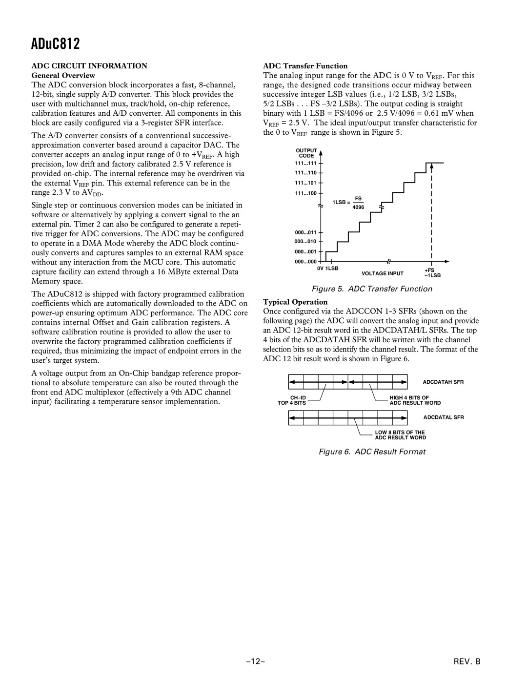
ADC Transfer Function
The analog input range for the ADC is 0 V to VREF. For this range, the designed code transitions occur midway between
successive integer LSB values (i.e., 1/2 LSB, 3/2 LSBs, 5/2 LSBs . . . FS
OUTPUT |
|
|
CODE |
|
|
111...111 |
|
|
111...110 |
|
|
111...101 |
|
|
111...100 | FS |
|
1LSB = |
| |
| 4096 |
|
000...011 |
|
|
000...010 |
|
|
000...001 |
|
|
000...000 |
|
|
0V 1LSB | VOLTAGE INPUT | +FS |
| ||
|
|
Figure 5. ADC Transfer Function
Typical Operation
Once configured via the ADCCON
ADCDATAH SFR
HIGH 4 BITS OF | |
TOP 4 BITS | ADC RESULT WORD |
ADCDATAL SFR
LOW 8 BITS OF THE
ADC RESULT WORD
Figure 6. ADC Result Format
REV. B |