| 3 | |
– V | 2 | |
VOLTAGE | ||
| ||
OUTPUT | 1 | |
|
0
0 | 5 | 10 | 15 |
SOURCE/SINK CURRENT – mA
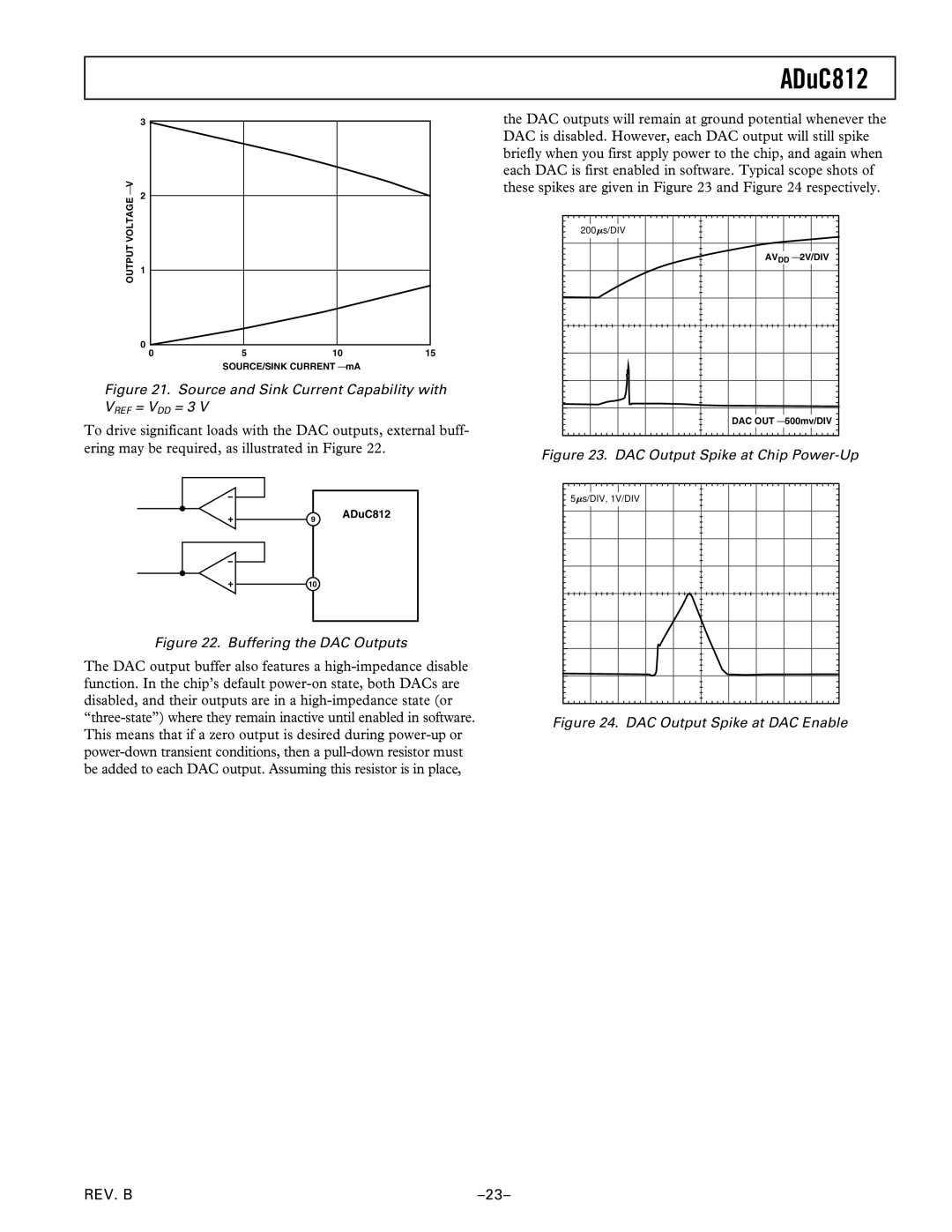
Figure 21. Source and Sink Current Capability with VREF = VDD = 3 V
To drive significant loads with the DAC outputs, external buff- ering may be required, as illustrated in Figure 22.
ADuC812
the DAC outputs will remain at ground potential whenever the DAC is disabled. However, each DAC output will still spike briefly when you first apply power to the chip, and again when each DAC is first enabled in software. Typical scope shots of these spikes are given in Figure 23 and Figure 24 respectively.
200 | s/DIV |
| AVDD – 2V/DIV |
| DAC OUT – 500mv/DIV |
Figure 23. DAC Output Spike at Chip Power-Up
9 | ADuC812 |
|
10
Figure 22. Buffering the DAC Outputs
The DAC output buffer also features a
5 s/DIV, 1V/DIV
Figure 24. DAC Output Spike at DAC Enable
REV. B |