ADuC812
|
|
|
|
|
|
| DOWNLOAD/DEBUG |
|
|
| ||
|
|
|
|
|
|
| ENABLE JUMPER |
|
|
| ||
|
|
|
|
|
|
| (NORMALLY OPEN) |
|
|
| ||
|
|
|
| DVDD | 1k |
| DV | DD |
| |||
|
|
|
|
|
|
|
|
|
|
| ||
|
|
|
|
|
|
|
|
| 1k |
|
|
|
|
|
|
|
|
|
|
|
|
|
|
| |
|
|
|
|
|
|
|
|
|
|
|
| EMULATION ACCESS |
| 52 | 51 | 50 | 49 48 |
| 47 46 | 45 44 43 | 42 41 | 40 |
|
| (NORMALLY OPEN) |
| 51 |
|
| DV |
| DGND |
| PSEN | EA |
|
|
|
ANALOG INPUT | ADC0 |
| DD |
|
|
|
| 39 |
| |||
|
|
|
|
|
|
|
| |||||
|
|
|
|
|
|
|
|
|
| 38 |
| |
|
|
|
|
|
|
|
|
|
| 37 |
| |
| AVDD |
|
|
|
|
|
|
|
| 36 | DVDD | |
| AVDD |
|
|
|
|
| DGND 35 |
| ||||
| AGND |
|
|
| ADuC812 | DVDD 34 |
| |||||
VREF OUTPUT | CREF |
|
|
|
|
| XTAL2 33 | 11.0592MHz | ||||
VREF |
|
|
|
|
| XTAL1 32 | ||||||
|
|
|
|
|
|
| ||||||
| DAC0 |
|
|
|
|
|
|
| 31 |
| ||
| DAC1 |
|
|
|
|
|
|
| 30 |
| ||
DAC OUTPUT | ADC7 | RESET | RxD | TxD |
| DV | DGND |
|
| 29 |
| |
|
|
|
|
|
|
| ||||||
|
|
|
|
|
| DD |
|
|
| 28 |
| |
|
|
|
|
|
|
|
|
|
|
| ||
|
|
|
|
|
|
|
|
|
| 27 |
| |
DVDD | ADM810 |
|
|
|
|
|
|
|
|
|
|
|
|
|
|
|
|
|
| NOT CONNECTED IN THIS EXAMPLE | |||||
VCC | RST |
|
|
| DVDD |
| ||||||
|
|
|
|
|
|
|
|
| ||||
GND |
|
|
|
ADM202 | DVDD | ||
C1+ | VCC |
| FEMALE |
V+ | GND |
| 1 |
C1– | T1OUT |
| 2 |
C2+ | R1IN |
| 3 |
C2– | R1OUT |
| 4 |
V– | T1IN |
| 5 |
T2OUT | T2IN |
| 6 |
R2IN | R2OUT |
| 7 |
|
|
| 8 |
|
|
| 9 |
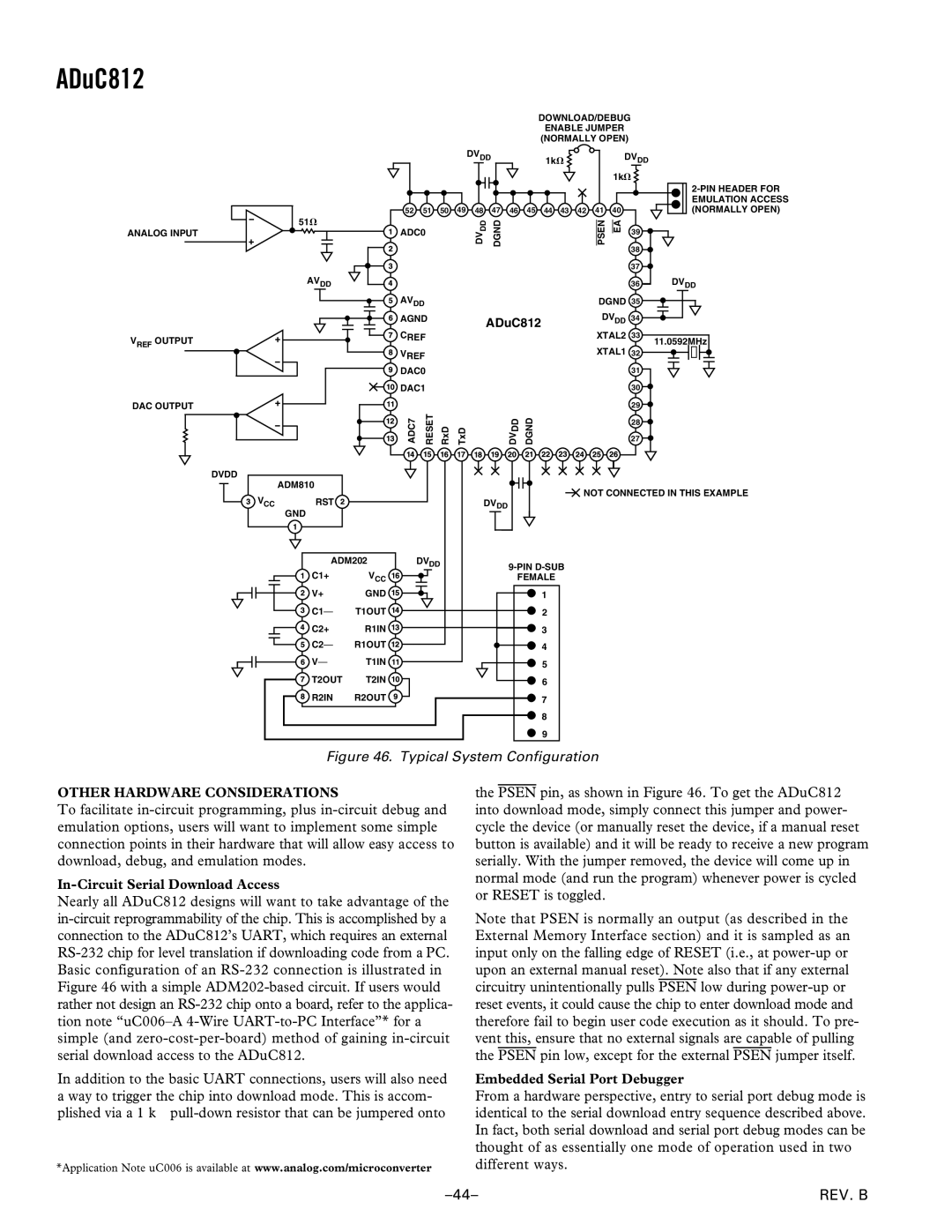
Figure 46. Typical System Configuration
OTHER HARDWARE CONSIDERATIONS
To facilitate
In-Circuit Serial Download Access
Nearly all ADuC812 designs will want to take advantage of the
In addition to the basic UART connections, users will also need a way to trigger the chip into download mode. This is accom- plished via a 1 kΩ
*Application Note uC006 is available at www.analog.com/microconverter
the PSEN pin, as shown in Figure 46. To get the ADuC812 into download mode, simply connect this jumper and power- cycle the device (or manually reset the device, if a manual reset button is available) and it will be ready to receive a new program serially. With the jumper removed, the device will come up in normal mode (and run the program) whenever power is cycled or RESET is toggled.
Note that PSEN is normally an output (as described in the External Memory Interface section) and it is sampled as an input only on the falling edge of RESET (i.e., at
Embedded Serial Port Debugger
From a hardware perspective, entry to serial port debug mode is identical to the serial download entry sequence described above. In fact, both serial download and serial port debug modes can be thought of as essentially one mode of operation used in two different ways.
REV. B |
