ADuC812
Driving the A/D Converter
The ADC incorporates a successive approximation (SAR) archi- tecture involving a
AIN0 | TEMPERATURE | ADuC812 | |
| SENSOR |
| |
AIN7 |
|
|
|
| 200 |
|
|
| TRACK |
|
|
| SW1 |
| CAPACITOR |
|
|
| |
| HOLD |
| DAC |
| 2pF |
| |
|
|
| |
|
| NODE A |
|
|
| SW2 |
|
| TRACK | HOLD | COMPARATOR |
|
|
| |
AGND |
|
|
|
Figure 7. Internal ADC Structure
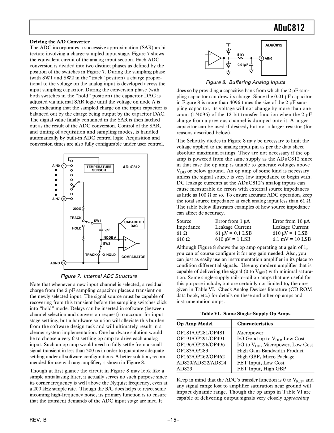
Note that whenever a new input channel is selected, a residual charge from the 2 pF sampling capacitor places a transient on the newly selected input. The signal source must be capable of recovering from this transient before the sampling switches click into “hold” mode. Delays can be inserted in software (between channel selection and conversion request) to account for input stage settling, but a hardware solution will alleviate this burden from the software design task and will ultimately result in a cleaner system implementation. One hardware solution would be to choose a very fast settling op amp to drive each analog input. Such an op amp would need to fully settle from a small signal transient in less than 300 ns in order to guarantee adequate settling under all software configurations. A better solution, recom- mended for use with any amplifier, is shown in Figure 8.
Though at first glance the circuit in Figure 8 may look like a simple antialiasing filter, it actually serves no such purpose since its corner frequency is well above the Nyquist frequency, even at a 200 kHz sample rate. Though the R/C does helps to reject some incoming
ADuC812
51
1 AIN0
0.01 F ![]()
Figure 8. Buffering Analog Inputs
does so by providing a capacitive bank from which the 2 pF sam- pling capacitor can draw its charge. Since the 0.01 ∝F capacitor in Figure 8 is more than 4096 times the size of the 2 pF sam- pling capacitor, its voltage will not change by more than one count (1/4096) of the
The Schottky diodes in Figure 8 may be necessary to limit the voltage applied to the analog input pin as per the data sheet absolute maximum ratings. They are not necessary if the op amp is powered from the same supply as the ADuC812 since in that case the op amp is unable to generate voltages above VDD or below ground. An op amp of some kind is necessary unless the signal source is very low impedance to begin with. DC leakage currents at the ADuC812’s analog inputs can cause measurable dc errors with external source impedances as little as 100 Ω or so. To ensure accurate ADC operation, keep the total source impedance at each analog input less than 61 Ω. The table below illustrates examples of how source impedance can affect dc accuracy.
Source | Error from 1 ∝A | Error from 10 ∝A |
Impedance | Leakage Current | Leakage Current |
61 Ω | 61 ∝V = 0.1 LSB | 610 ∝V = 1 LSB |
610 Ω | 610 ∝V = 1 LSB | 6.1 mV = 10 LSB |
Although Figure 8 shows the op amp operating at a gain of 1, you can of course configure it for any gain needed. Also, you can just as easily use an instrumentation amplifier in its place to condition differential signals. Use any modern amplifier that is capable of delivering the signal (0 to VREF) with minimal satura- tion. Some
Table VI. Some Single-Supply Op Amps
Op Amp Model | Characteristics |
|
|
OP181/OP281/OP481 | Micropower |
OP191/OP291/OP491 | I/O Good up to VDD, Low Cost |
OP196/OP296/OP496 | I/O to VDD, Micropower, Low Cost |
OP183/OP283 | High |
OP162/OP262/OP462 | High GBP, Micro Package |
AD820/AD822/AD824 | FET Input, Low Cost |
AD823 | FET Input, High GBP |
|
|
Keep in mind that the ADC’s transfer function is 0 to VREF, and any signal range lost to amplifier saturation near ground will impact dynamic range. Though the op amps in Table VI are capable of delivering output signals very closely approaching
REV. B |