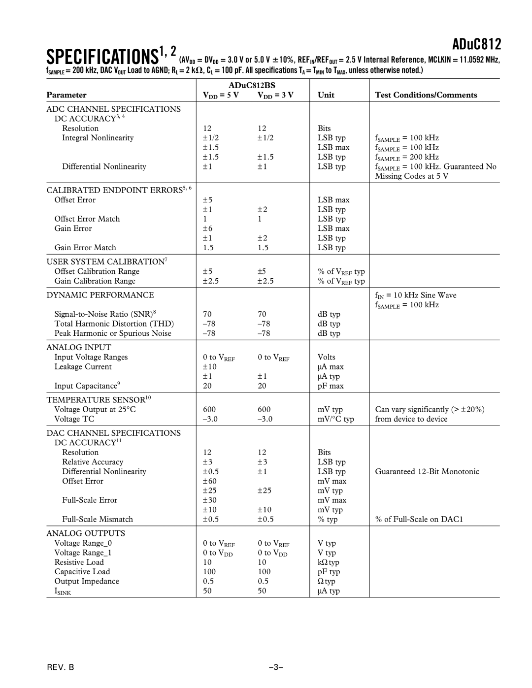
SPECIFICATIONS1, 2 |
|
|
|
| ADuC812 | |
(AVDD = DVDD = 3.0 V or 5.0 V 10%, REFIN/REFOUT = 2.5 V Internal Reference, MCLKIN = 11.0592 MHz, | ||||||
fSAMPLE = 200 kHz, DAC VOUT Load to AGND; RL = 2 k , CL = 100 pF. All specifications TA = TMIN to TMAX, unless otherwise noted.) | ||||||
|
| ADuC812BS |
|
|
| |
Parameter |
| VDD = 5 V | VDD = 3 V | Unit | Test Conditions/Comments | |
ADC CHANNEL SPECIFICATIONS |
|
|
|
|
| |
DC ACCURACY3, 4 |
|
|
|
|
|
|
Resolution |
| 12 | 12 | Bits |
|
|
Integral Nonlinearity |
| ± 1/2 | ± 1/2 | LSB typ | fSAMPLE = 100 kHz | |
|
| ± 1.5 |
| LSB max | fSAMPLE = 100 kHz | |
|
| ± 1.5 | ± 1.5 | LSB typ | fSAMPLE = 200 kHz | |
Differential Nonlinearity |
| ± 1 | ± 1 | LSB typ | fSAMPLE = 100 kHz. Guaranteed No | |
|
|
|
|
| Missing Codes at 5 V | |
|
|
|
|
|
| |
CALIBRATED ENDPOINT ERRORS5, 6 | ± 5 |
|
|
|
| |
Offset Error |
|
| LSB max |
|
| |
|
| ± 1 | ± 2 | LSB typ |
|
|
Offset Error Match |
| 1 | 1 | LSB typ |
|
|
Gain Error |
| ± 6 |
| LSB max |
|
|
|
| ± 1 | ± 2 | LSB typ |
|
|
Gain Error Match |
| 1.5 | 1.5 | LSB typ |
|
|
|
|
|
|
|
|
|
USER SYSTEM CALIBRATION7 |
| ± 5 | ±5 |
|
|
|
Offset Calibration Range |
| % of VREF typ |
|
| ||
Gain Calibration Range |
| ± 2.5 | ± 2.5 | % of VREF typ |
|
|
DYNAMIC PERFORMANCE |
|
|
|
| fIN = 10 kHz Sine Wave | |
| 70 | 70 | dB typ | fSAMPLE = 100 kHz | ||
|
|
| ||||
Total Harmonic Distortion (THD) |
| dB typ |
|
| ||
Peak Harmonic or Spurious Noise |
| dB typ |
|
| ||
|
|
|
|
|
|
|
ANALOG INPUT |
|
|
|
|
|
|
Input Voltage Ranges |
| 0 to VREF | 0 to VREF | Volts |
|
|
Leakage Current |
| ± 10 |
| ∝A max |
|
|
Input Capacitance9 |
| ± 1 | ± 1 | ∝A typ |
|
|
| 20 | 20 | pF max |
|
| |
TEMPERATURE SENSOR10 |
|
|
|
|
|
|
Voltage Output at 25°C |
| 600 | 600 | mV typ | Can vary significantly (> ± 20%) | |
Voltage TC |
| mV/°C typ | from device to device | |||
|
|
|
|
|
| |
DAC CHANNEL SPECIFICATIONS |
|
|
|
|
| |
DC ACCURACY11 |
|
|
|
|
|
|
Resolution |
| 12 | 12 | Bits |
|
|
Relative Accuracy |
| ± 3 | ± 3 | LSB typ |
|
|
Differential Nonlinearity |
| ± 0.5 | ± 1 | LSB typ | Guaranteed | |
Offset Error |
| ± 60 |
| mV max |
|
|
|
| ± 25 | ± 25 | mV typ |
|
|
| ± 30 |
| mV max |
|
| |
|
| ± 10 | ± 10 | mV typ |
|
|
| ± 0.5 | ± 0.5 | % typ | % of | ||
|
|
|
|
|
|
|
ANALOG OUTPUTS |
|
|
|
|
|
|
Voltage Range_0 |
| 0 to VREF | 0 to VREF | V typ |
|
|
Voltage Range_1 |
| 0 to VDD | 0 to VDD | V typ |
|
|
Resistive Load |
| 10 | 10 | kΩ typ |
|
|
Capacitive Load |
| 100 | 100 | pF typ |
|
|
Output Impedance |
| 0.5 | 0.5 | Ω typ |
|
|
ISINK |
| 50 | 50 | ∝A typ |
|
|
REV. B |