ADuC812
TIMING SPECIFICATIONS1, 2, 3
(AVDD = DVDD = 3.0 V or 5.0 V 10%. All specifications TA = TMIN to TMAX unless otherwise noted.)
|
|
| 12 MHz |
| Variable Clock |
|
| ||
Parameter |
| Min | Typ | Max | Min | Typ | Max | Unit | Figure |
|
|
|
|
|
|
|
|
| |
CLOCK INPUT (External Clock Driven XTAL1) |
|
|
|
|
|
|
|
| |
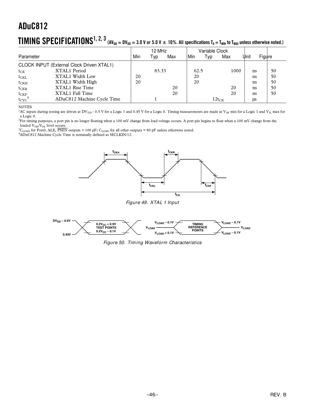
tCK | XTAL1 Period |
| 83.33 |
| 62.5 |
| 1000 | ns | 50 |
tCKL | XTAL1 Width Low | 20 |
|
| 20 |
|
| ns | 50 |
tCKH | XTAL1 Width High | 20 |
|
| 20 |
|
| ns | 50 |
tCKR | XTAL1 Rise Time |
|
| 20 |
|
| 20 | ns | 50 |
tCKF | XTAL1 Fall Time |
|
| 20 |
|
| 20 | ns | 50 |
4 | ADuC812 Machine Cycle Time |
| 1 |
|
| 12tCK |
| ∝s |
|
tCYC |
|
|
|
|
| ||||
NOTES
1AC inputs during testing are driven at DVDD – 0.5 V for a Logic 1 and 0.45 V for a Logic 0. Timing measurements are made at V IH min for a Logic 1 and VIL max for a Logic 0.
2For timing purposes, a port pin is no longer floating when a 100 mV change from load voltage occurs. A port pin begins to float when a 100 mV change from the loaded VOH/VOL level occurs.
3CLOAD for Port0, ALE, PSEN outputs = 100 pF; CLOAD for all other outputs = 80 pF unless otherwise noted.
4ADuC812 Machine Cycle Time is nominally defined as MCLKIN/12.
|
|
| tCKH |
|
|
|
|
|
| tCKR |
|
| |
|
|
|
|
|
|
|
|
|
|
| |||
|
|
|
|
|
|
|
|
|
|
|
|
|
|
|
|
|
|
|
|
|
|
|
|
|
|
|
|
|
|
|
|
|
|
|
|
|
|
|
|
|
|
|
|
|
|
|
|
|
|
|
|
|
|
|
|
|
|
|
|
|
|
|
|
|
|
|
|
|
|
tCKL
tCK
Figure 49. XTAL 1 Input
tCKF
DVDD – 0.5V |
|
|
|
|
|
|
|
|
| VLOAD – 0.1V |
|
|
|
|
| VLOAD – 0.1V | ||||
|
|
|
|
|
|
|
|
|
|
|
| |||||||||
|
|
|
|
| 0.2VCC + 0.9V |
|
|
|
|
| TIMING |
| ||||||||
|
|
|
|
| TEST POINTS |
|
|
| VLOAD |
|
|
|
| REFERENCE |
|
|
| VLOAD | ||
|
|
|
|
|
|
|
|
|
| |||||||||||
|
|
|
|
| 0.2VCC – 0.1V |
|
|
| VLOAD + 0.1V |
|
| POINTS |
| VLOAD – 0.1V | ||||||
0.45V |
|
|
|
|
|
|
|
|
|
|
|
|
|
| ||||||
|
|
|
|
|
|
|
| |||||||||||||
Figure 50. Timing Waveform Characteristics
REV. B |