ADuC812
USER INTERFACE TO OTHER
PERIPHERALS
The following section gives a brief overview of the various peripherals also available
DAC
The ADuC812 incorporates two
Each can operate in
DACCON | DAC Control Register |
SFR Address | FDH |
04H | |
Bit Addressable | No |
MODE
RNG1
RNG0
CLR1
CLR0
SYNC
PD1
PD0
|
|
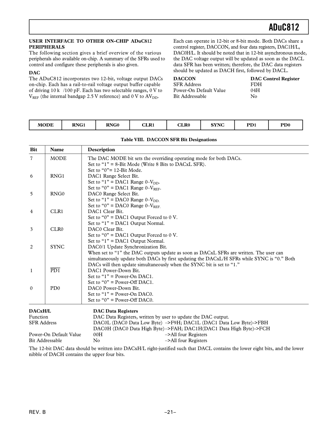
| Table VIII. DACCON SFR Bit Designations | |
|
|
|
|
|
Bit |
| Name | Description |
|
|
|
|
| |
7 |
| MODE | The DAC MODE bit sets the overriding operating mode for both DACs. | |
|
|
| Set to “1” = | |
|
|
| Set to “0”= |
|
6 |
| RNG1 | DAC1 Range Select Bit. |
|
|
|
| Set to “1” = DAC1 Range |
|
|
|
| Set to “0” = DAC1 Range |
|
5 |
| RNG0 | DAC0 Range Select Bit. |
|
|
|
| Set to “1” = DAC0 Range |
|
|
|
| Set to “0” = DAC0 Range |
|
4 |
| CLR1 | DAC1 Clear Bit. |
|
|
|
| Set to “0” = DAC1 Output Forced to 0 V. | |
|
|
| Set to “1” = DAC1 Output Normal. |
|
3 |
| CLR0 | DAC0 Clear Bit. |
|
|
|
| Set to “0” = DAC1 Output Forced to 0 V. | |
|
|
| Set to “1” = DAC1 Output Normal. |
|
2 |
| SYNC | DAC0/1 Update Synchronization Bit. | |
|
|
| When set to “1” the DAC outputs update as soon as DACxL SFRs are written. The user can | |
|
|
| simultaneously update both DACs by first updating the DACxL/H SFRs while SYNC is “0.” Both | |
|
|
| DACs will then update simultaneously when the SYNC bit is set to “1.” | |
1 |
| PD1 | DAC1 |
|
|
|
| Set to “1” = |
|
|
|
| Set to “0” = |
|
0 |
| PD0 | DAC0 |
|
|
|
| Set to “1” = |
|
|
|
| Set to “0” = |
|
|
|
|
| |
DACxH/L | DAC Data Registers |
| ||
Function |
| DAC Data Registers, written by user to update the DAC output. | ||
SFR Address | DAC0L (DAC0 Data Low Byte) | |||
|
|
| DAC0H (DAC0 Data High Byte) | |
00H | ||||
Bit Addressable | No | |||
The
REV. B |
