ADuC812
OVERVIEW OF MCU-RELATED SFRs
Accumulator SFR
ACC is the Accumulator register and is used for math opera- tions including addition, subtraction, integer multiplication and division, and Boolean bit manipulations. The mnemonics for
B SFR
The B register is used with the ACC for multiplication and division operations. For other instructions it can be treated as a
Stack Pointer SFR
The SP register is the stack pointer and is used to hold an inter- nal RAM address that is called the “top of the stack.” The SP register is incremented before data is stored during PUSH and CALL executions. While the Stack may reside anywhere in
Data Pointer
The Data Pointer is made up of three
Program Status Word SFR
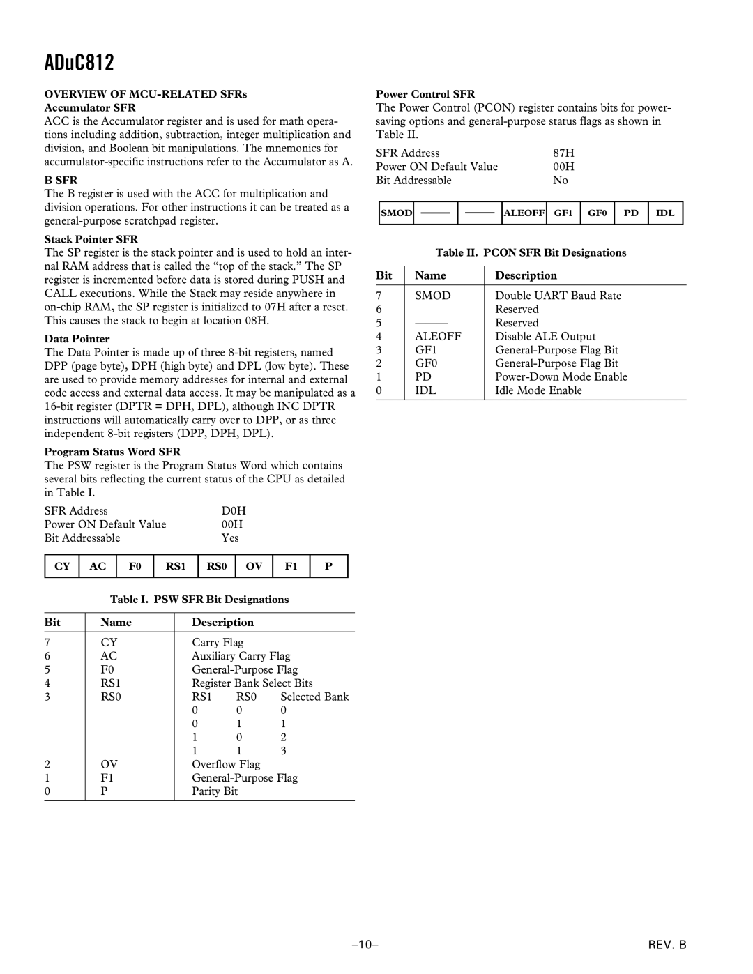
The PSW register is the Program Status Word which contains several bits reflecting the current status of the CPU as detailed in Table I.
SFR Address |
|
|
|
| D0H |
|
|
|
| ||||
Power ON Default Value |
|
| 00H |
|
|
|
| ||||||
Bit Addressable |
|
|
|
| Yes |
|
|
|
| ||||
|
|
|
|
|
|
|
|
|
|
|
|
| |
CY |
| AC |
| F0 | RS1 | RS0 | OV | F1 |
| P |
| ||
|
|
|
|
|
|
|
|
|
|
|
| ||
|
| Table I. PSW SFR Bit Designations |
|
| |||||||||
|
|
|
|
|
|
|
|
| |||||
Bit |
| Name |
| Description |
|
|
|
| |||||
|
|
|
|
|
|
|
|
|
| ||||
7 |
| CY |
|
| Carry Flag |
|
|
|
| ||||
6 |
| AC |
|
| Auxiliary Carry Flag |
|
| ||||||
5 |
| F0 |
|
|
|
| |||||||
4 |
| RS1 |
|
| Register Bank Select Bits |
|
| ||||||
3 |
| RS0 |
|
| RS1 |
| RS0 | Selected Bank | |||||
|
|
|
|
|
| 0 |
| 0 | 0 |
|
|
| |
|
|
|
|
|
| 0 |
| 1 | 1 |
|
|
| |
|
|
|
|
|
| 1 |
| 0 | 2 |
|
|
| |
|
|
|
|
|
| 1 |
| 1 | 3 |
|
|
| |
2 |
| OV |
|
| Overflow Flag |
|
|
|
| ||||
1 |
| F1 |
|
|
|
| |||||||
0 |
| P |
|
| Parity Bit |
|
|
|
| ||||
|
|
|
|
|
|
|
|
|
|
|
|
|
|
Power Control SFR
The Power Control (PCON) register contains bits for power- saving options and
SFR Address |
|
|
|
| 87H |
| ||||||||||
Power ON Default Value | 00H |
| ||||||||||||||
Bit Addressable |
|
|
|
| No |
| ||||||||||
|
|
|
|
|
|
|
|
|
|
|
|
|
|
|
|
|
| SMOD |
|
|
|
|
|
|
|
| ALEOFF | GF1 | GF0 | PD | IDL |
| |
|
|
|
|
|
|
|
|
|
| |||||||
|
|
|
|
|
|
|
|
|
|
|
|
|
|
|
|
|
|
|
|
| Table II. PCON SFR Bit Designations |
| |||||||||||
|
|
|
|
|
|
|
|
|
|
| ||||||
Bit |
| Name |
| Description |
| |||||||||||
|
|
|
|
|
|
|
|
|
|
| ||||||
7 |
| SMOD |
| Double UART Baud Rate |
| |||||||||||
6 |
|
| Reserved |
|
|
|
|
| ||||||||
5 |
|
| Reserved |
|
|
|
|
| ||||||||
4 |
| ALEOFF |
| Disable ALE Output |
| |||||||||||
3 |
| GF1 |
|
| ||||||||||||
2 |
| GF0 |
|
| ||||||||||||
1 |
| PD |
|
| ||||||||||||
0 |
| IDL |
| Idle Mode Enable |
| |||||||||||
|
|
|
|
|
|
|
|
|
|
|
|
|
|
|
|
|
REV. B |