ADuC812
ABSOLUTE MAXIMUM RATINGS* (TA = 25°C unless otherwise noted)
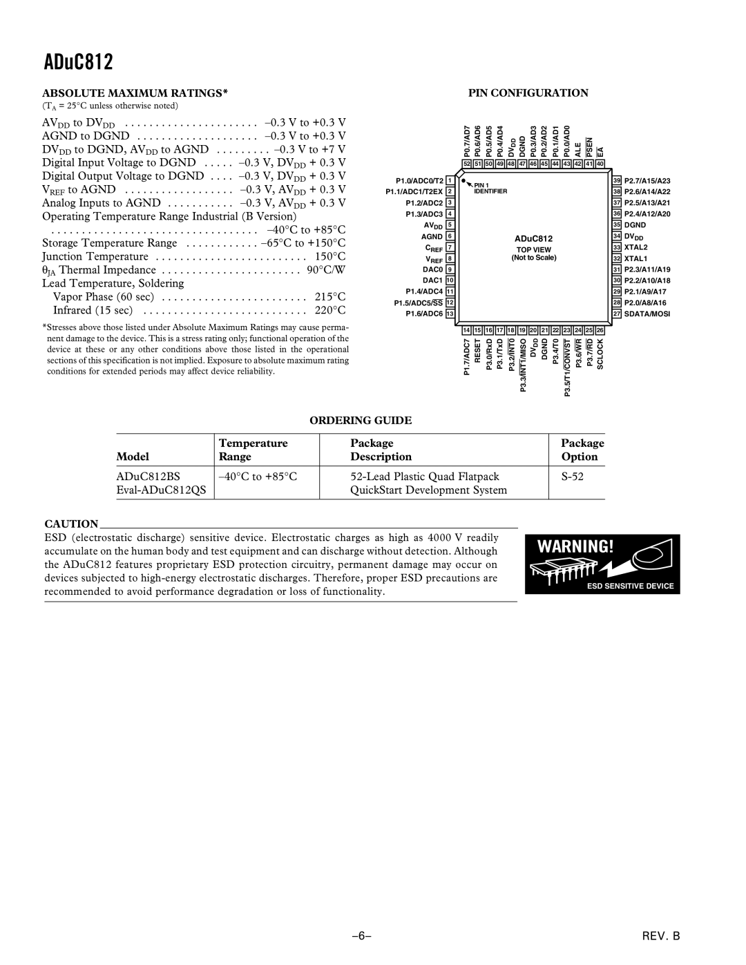
PIN CONFIGURATION
AVDD to DVDD | . . . |
AGND to DGND | . . . |
DVDD to DGND, AVDD to AGND . . . . | . . . . . |
Digital Input Voltage to DGND | |
Digital Output Voltage to DGND . . . . | |
VREF to AGND | |
Analog Inputs to AGND | |
Operating Temperature Range Industrial (B Version) | |
. . . . . . . . . . . . . . . . . . . . . . . . . . . . . . . | . . . |
Storage Temperature Range | . . . |
Junction Temperature | . . . . . . . . . . . 150°C |
θJA Thermal Impedance | . . . . . . . . . . 90°C/W |
Lead Temperature, Soldering | . . . . . . . . . . . 215°C |
Vapor Phase (60 sec) | |
Infrared (15 sec) | . . . . . . . . . . . 220°C |
*Stresses above those listed under Absolute Maximum Ratings may cause perma- nent damage to the device. This is a stress rating only; functional operation of the device at these or any other conditions above those listed in the operational sections of this specification is not implied. Exposure to absolute maximum rating conditions for extended periods may affect device reliability.
P1.0/ADC0/T2 1
P1.1/ADC1/T2EX 2
P1.2/ADC2 3
P1.3/ADC3 4
AVDD 5
AGND 6
CREF 7
VREF 8
DAC0 9
DAC1 10
P1.4/ADC4 11
P1.5/ADC5/SS 12
P1.6/ADC6 13
P0.7/AD7 | P0.6/AD6 | P0.5/AD5 | P0.4/AD4 | DV | DGND | P0.3/AD3 | P0.2/AD2 | P0.1/AD1 | P0.0/AD0 | ALE | PSEN | EA |
|
|
|
| DD |
|
|
|
|
|
|
|
|
|
|
|
|
|
|
|
|
|
|
|
|
|
52 | 51 | 50 | 49 | 48 | 47 | 46 | 45 | 44 | 43 | 42 | 41 | 40 |
![]() PIN 1
PIN 1
IDENTIFIER
ADuC812
TOP VIEW
(Not to Scale)
14 | 15 | 16 | 17 | 18 | 19 | 20 | 21 | 22 | 23 | 24 | 25 | 26 |
P1.7/ADC7 | RESET | P3.0/RxD | P3.1/TxD | P3.2/INT0 | P3.3/INT1/MISO | DD | DGND | P3.4/T0 | P3.5/T1/CONVST | P3.6/WR | P3.7/RD | SCLOCK |
DV |
39P2.7/A15/A23
38P2.6/A14/A22
37P2.5/A13/A21
36P2.4/A12/A20
35DGND
34DVDD
33XTAL2
32XTAL1
31P2.3/A11/A19
30P2.2/A10/A18
29P2.1/A9/A17
28P2.0/A8/A16
27SDATA/MOSI
ORDERING GUIDE
| Temperature | Package | Package |
Model | Range | Description | Option |
|
|
|
|
ADuC812BS | |||
| QuickStart Development System |
| |
|
|
|
|
CAUTION
ESD (electrostatic discharge) sensitive device. Electrostatic charges as high as 4000 V readily accumulate on the human body and test equipment and can discharge without detection. Although the ADuC812 features proprietary ESD protection circuitry, permanent damage may occur on devices subjected to
WARNING! |
ESD SENSITIVE DEVICE |
REV. B |