ADuC812
Table XII. SPICON SFR Bit Designations (continued)
Bit | Name | Description |
| |
|
|
| ||
1 | SPR1 | SPI | ||
0 | SPR0 | These bits select the SCLOCK rate | ||
|
| SPR1 | SPR0 | Selected Bit Rate |
|
| 0 | 0 | fOSC/4 |
|
| 0 | 1 | fOSC/8 |
|
| 1 | 0 | fOSC/32 |
|
| 1 | 1 | fosc/64 |
|
| In SPI Slave Mode, i.e., SPIM = 0, the logic level on the external SS pin (Pin #12) | ||
|
| can be read via the SPR0 bit. | ||
|
|
|
|
|
NOTE
The CPOL and CPHA bits should both contain the same values for master and slave devices.
SPIDAT | SPI Data Register |
Function | The SPIDAT SFR is written by the |
| user to transmit data over the SPI |
| interface or read by user code to |
| read data just received by the SPI |
| interface. |
SFR Address | F7H |
00H | |
Bit Addressable | No |
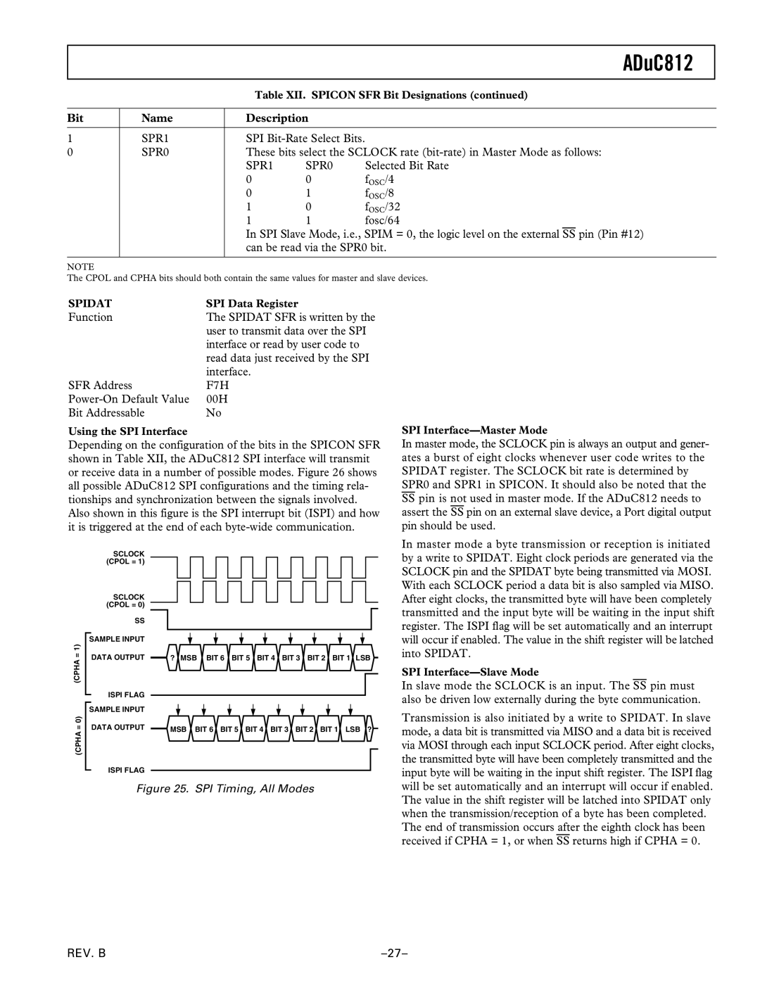
Using the SPI Interface
Depending on the configuration of the bits in the SPICON SFR shown in Table XII, the ADuC812 SPI interface will transmit or receive data in a number of possible modes. Figure 26 shows all possible ADuC812 SPI configurations and the timing rela- tionships and synchronization between the signals involved. Also shown in this figure is the SPI interrupt bit (ISPI) and how it is triggered at the end of each
SCLOCK (CPOL = 1)
SCLOCK (CPOL = 0)
SS
SAMPLE INPUT |
|
=1) | ? MSB BIT 6 BIT 5 BIT 4 BIT 3 BIT 2 BIT 1 LSB |
DATA OUTPUT | |
(CPHA |
|
ISPI FLAG |
|
SAMPLE INPUT |
|
=0) | MSB BIT 6 BIT 5 BIT 4 BIT 3 BIT 2 BIT 1 LSB ? |
DATA OUTPUT | |
(CPHA |
|
ISPI FLAG
Figure 25. SPI Timing, All Modes
SPI
In master mode, the SCLOCK pin is always an output and gener- ates a burst of eight clocks whenever user code writes to the SPIDAT register. The SCLOCK bit rate is determined by SPR0 and SPR1 in SPICON. It should also be noted that the
SSpin is not used in master mode. If the ADuC812 needs to assert the SS pin on an external slave device, a Port digital output pin should be used.
In master mode a byte transmission or reception is initiated by a write to SPIDAT. Eight clock periods are generated via the SCLOCK pin and the SPIDAT byte being transmitted via MOSI. With each SCLOCK period a data bit is also sampled via MISO. After eight clocks, the transmitted byte will have been completely transmitted and the input byte will be waiting in the input shift register. The ISPI flag will be set automatically and an interrupt will occur if enabled. The value in the shift register will be latched into SPIDAT.
SPI
In slave mode the SCLOCK is an input. The SS pin must also be driven low externally during the byte communication.
Transmission is also initiated by a write to SPIDAT. In slave mode, a data bit is transmitted via MISO and a data bit is received via MOSI through each input SCLOCK period. After eight clocks, the transmitted byte will have been completely transmitted and the input byte will be waiting in the input shift register. The ISPI flag will be set automatically and an interrupt will occur if enabled. The value in the shift register will be latched into SPIDAT only when the transmission/reception of a byte has been completed.
The end of transmission occurs after the eighth clock has been received if CPHA = 1, or when SS returns high if CPHA = 0.
REV. B |