ADuC812
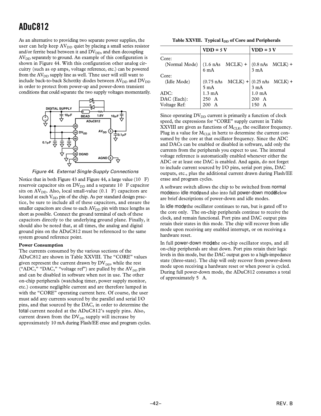
As an alternative to providing two separate power supplies, the user can help keep AVDD quiet by placing a small series resistor and/or ferrite bead between it and DVDD, and then decoupling AVDD separately to ground. An example of this configuration is shown in Figure 44. With this configuration other analog cir- cuitry (such as op amps, voltage reference, etc.) can be powered from the AVDD supply line as well. Thne user will still want to include
DIGITAL SUPPLY |
|
|
| |
+ | 10 F | BEAD | 1.6V | 10 F |
– |
| ADuC812 |
| |
|
|
| ||
| 20 |
|
|
|
| 34 | DVDD | AVDD | 5 |
|
|
|
| 0.1 F |
| 48 |
|
|
|
0.1 | F |
|
|
|
| 21 |
|
|
|
| 35 | DGND |
|
|
| 47 |
| AGND 6 | |
|
|
|
| |
Figure 44. External Single-Supply Connections
Notice that in both Figure 43 and Figure 44, a large value (10 ∝F) reservoir capacitor sits on DVDD and a separate 10 ∝F capacitor sits on AVDD. Also, local
Power Consumption
The currents consumed by the various sections of the ADuC812 are shown in Table XXVIII. The “CORE” values given represent the current drawn by DVDD, while the rest (“ADC,” “DAC,” “voltage ref”) are pulled by the AVDD pin and can be disabled in software when not in use. The other
Table XXVIII. Typical IDD of Core and Peripherals
| VDD = 5 V | VDD = 3 V |
|
|
|
Core: | (1.6 nAs ⋅ MCLK) + | (0.8 nAs ⋅ MCLK) + |
(Normal Mode) | ||
| 6 mA | 3 mA |
Core: | (0.75 nAs ⋅ MCLK) + | (0.25 nAs ⋅ MCLK) + |
(Idle Mode) | ||
| 5 mA | 3 mA |
ADC: | 1.3 mA | 1.0 mA |
DAC (Each): | 250 ∝A | 200 ∝A |
Voltage Ref: | 200 ∝A | 150 ∝A |
|
|
|
Since operating DVDD current is primarily a function of clock speed, the expressions for “CORE” supply current in Table XXVIII are given as functions of MCLK, the oscillator frequency. Plug in a value for MCLK in hertz to determine the current con- sumed by the core at that oscillator frequency. Since the ADC and DACs can be enabled or disabled in software, add only the currents from the peripherals you expect to use. The internal voltage reference is automatically enabled whenever either the ADC or at least one DAC is enabled. And again, do not forget to include current sourced by I/O pins, serial port pins, DAC outputs, etc., plus the additional current drawn during Flash/EE erase and program cycles.
A software switch allows the chip to be switched from normal mode into idle mode, and also into full
In idle mode, the oscillator continues to run, but is gated off to the core only. The
In full
REV. B |