ADuC812
the gain calibration coefficient is divided into ADCGAINH (6 bits) and ADCGAINL (8 bits).The offset calibration coefficient compen- sates for dc offset errors in both the ADC and the input signal.
Increasing the offset coefficient compensates for positive offset, and effectively pushes the ADC Transfer Function DOWN. Decreasing the offset coefficient compensates for negative offset, and effectively pushes the ADC Transfer Function UP. The maximum offset that can be compensated is typically ± 5% of VREF, which equates to typically ± 125 mV with a 2.5 V reference.
Similarly, the gain calibration coefficient compensates for dc gain errors in both the ADC and the input signal.
Increasing the gain coefficient compensates for a smaller analog input signal range and scales the ADC Transfer Function UP, effectively increasing the slope of the transfer function. Decreas- ing the gain coefficient, compensates for a larger analog input signal range and scales the ADC Transfer Function DOWN, effectively decreasing the slope of the transfer function. The maximum analog input signal range for which the gain coeffi- cient can compensate is 1.025 ⋅ VREF and the minimum input range is 0.975 ⋅ VREF which equates to typically ± 2.5% of the reference voltage.
Calibration
Each ADuC812 is calibrated in the factory prior to shipping and the offset and gain calibration coefficients are stored in a hidden area of FLASH/EE memory. Each time the ADuC812 powers up, an internal
the SFR area.
The MicroConverter ADC accuracy may vary from system to system due to board layout, grounding, clock speed, etc. To get the best ADC accuracy in your system, you should perform the software calibration routine described in the technical note uC005 available from the MicroConverter home page (www.analog.com/microconverter).
NONVOLATILE FLASH MEMORY
Flash Memory Overview
The ADuC812 incorporates Flash memory technology
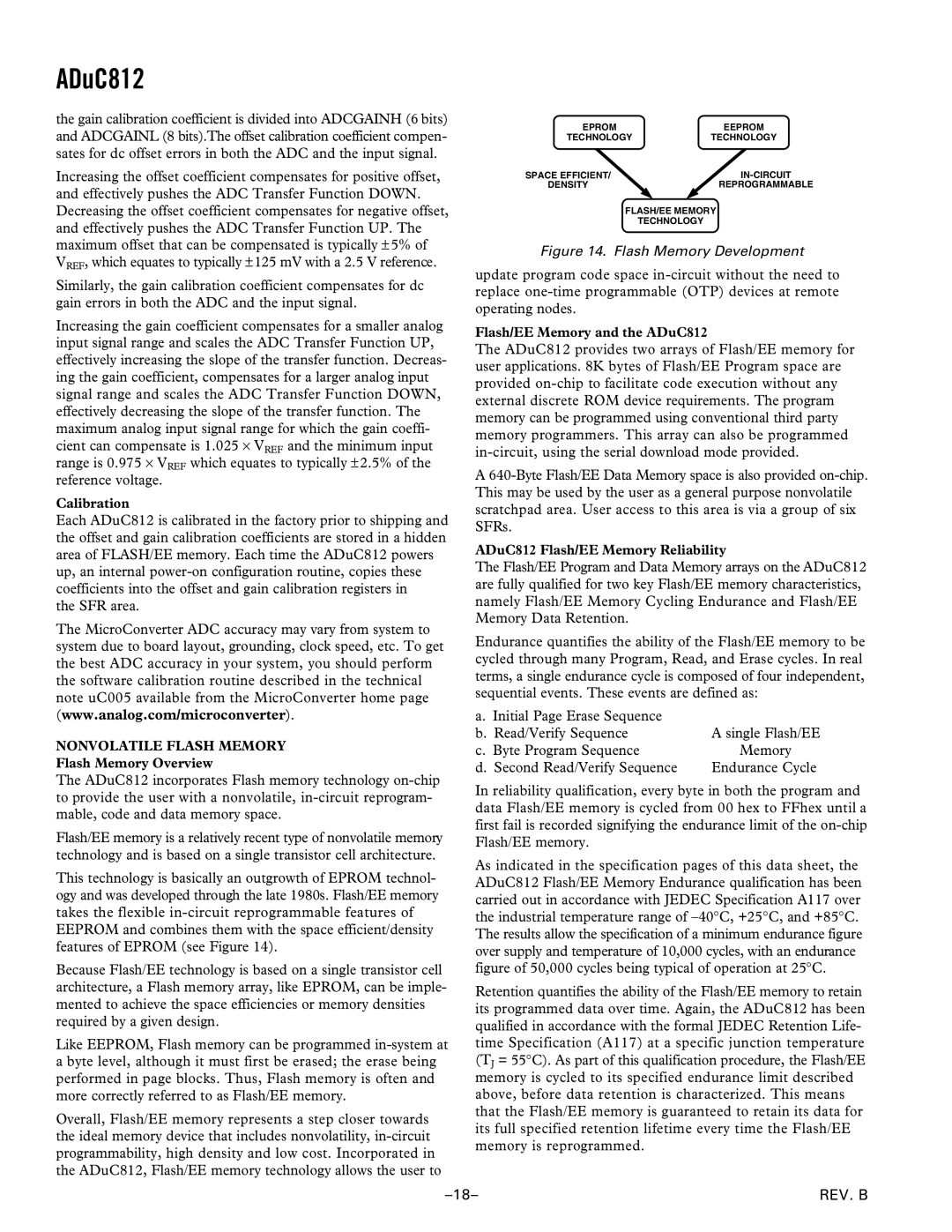
Flash/EE memory is a relatively recent type of nonvolatile memory technology and is based on a single transistor cell architecture.
This technology is basically an outgrowth of EPROM technol- ogy and was developed through the late 1980s. Flash/EE memory takes the flexible
Because Flash/EE technology is based on a single transistor cell architecture, a Flash memory array, like EPROM, can be imple- mented to achieve the space efficiencies or memory densities required by a given design.
Like EEPROM, Flash memory can be programmed
Overall, Flash/EE memory represents a step closer towards the ideal memory device that includes nonvolatility,
EPROM | EEPROM |
TECHNOLOGY | TECHNOLOGY |
SPACE EFFICIENT/ | |
DENSITY | REPROGRAMMABLE |
FLASH/EE MEMORY
TECHNOLOGY
Figure 14. Flash Memory Development
update program code space
Flash/EE Memory and the ADuC812
The ADuC812 provides two arrays of Flash/EE memory for user applications. 8K bytes of Flash/EE Program space are provided
A
ADuC812 Flash/EE Memory Reliability
The Flash/EE Program and Data Memory arrays on the ADuC812 are fully qualified for two key Flash/EE memory characteristics, namely Flash/EE Memory Cycling Endurance and Flash/EE Memory Data Retention.
Endurance quantifies the ability of the Flash/EE memory to be cycled through many Program, Read, and Erase cycles. In real terms, a single endurance cycle is composed of four independent, sequential events. These events are defined as:
a. Initial Page Erase Sequence |
|
b. Read/Verify Sequence | A single Flash/EE |
c. Byte Program Sequence | Memory |
d. Second Read/Verify Sequence | Endurance Cycle |
In reliability qualification, every byte in both the program and data Flash/EE memory is cycled from 00 hex to FFhex until a first fail is recorded signifying the endurance limit of the
As indicated in the specification pages of this data sheet, the ADuC812 Flash/EE Memory Endurance qualification has been carried out in accordance with JEDEC Specification A117 over the industrial temperature range of
Retention quantifies the ability of the Flash/EE memory to retain its programmed data over time. Again, the ADuC812 has been qualified in accordance with the formal JEDEC Retention Life- time Specification (A117) at a specific junction temperature (TJ = 55°C). As part of this qualification procedure, the Flash/EE memory is cycled to its specified endurance limit described above, before data retention is characterized. This means that the Flash/EE memory is guaranteed to retain its data for its full specified retention lifetime every time the Flash/EE memory is reprogrammed.
REV. B |