F2MC-8L
Page
Fujitsu Limited
Page
Trademark
Purpose of This Manual and Intended Reader
Fujitsu Limited
Structure of This Manual
This chapter describes the functions and operation of Uart
This appendix shows the I/O map and instructions list
Copyright 2005-2008 Fujitsu Limited All rights reserved Iii
Example notation of multi-use pins P33/EC pin
Reading this Manual
Contents
115
127
161
135
205
259
225
243
279
339
313
347
403
357
375
Appendix a
Changes For details, refer to main body
RST
Xii
Chapter Overview
Overview
Features of MB89202/F202RA Series
Uart
Wild registers
Low-power consumption modes standby modes
Up to 26 pins of I/O ports
KB Flash with read protection
MB89201 MB89F202/F202RA MB89V201
MB89202/F202RA Series Product Lineup
1 MB89202/F202RA Series Models
Cmos
PWM
Specification
2 CPU and Peripheral Functions of MB89202/F202RA Series
Uart
Package MB89201 MB89F202/F202RA MB89V202
Differences between Models
1 Differences between Models
Current consumption
Block Diagram of MB89202/F202RA Series
1 Block Diagram of MB89202/F202RA Series
Pin Assignment
1 Pin Assignment of DIP-32P-M06
Pin Assignment of FPT-34P-M03
2 Pin Assignment of FPT-34P-M03
Package Dimensions
Package Dimension of DIP-32P-M06
Package Dimension of FPT-34P-M03
Pin Functions Description 1/2
Pin Functions Description
Pin No Circuit Function Name Type
Pin Functions Description 2/2
I/O Circuit Types
Circuit Types 1/2 Remarks
Circuit Types 2/2
Types Circuit Remarks
Overview
Precautions on Handling Devices
Chapter Handling Devices
Precautions on Handling Devices
Handling Devices
Step-down circuit stabilization time
Product name Operating voltage Step-down circuit
Oscillation stabilization wait time 218/FCH
Chapter CPU
Area address 0000H to 007FH
Memory Space
CPU
RAM area
Memory Map
1 Vector /2
Specific-purpose Areas
Vector Table Area Address FFC0H to Ffffh
Address in the vector table
Fffd H
Fffb H
Fffe H Ffff H
Bit Operand Storage State
Location of 16-bit Data on Memory
Bit Data Storage State in Stack
Program counter PC
Dedicated Register
Functions of the Dedicated Register
Accumulator a
Extra-pointer EP
Temporary Accumulator T
Index register
Stack pointer SP
Condition Code Register CCR
Bits for Indicating Arithmetic Operation Results
1 Interrupt Levels
Bits for Controlling Acceptance of Interrupts
IL1 IL0
4 Configuration of Register Bank Pointer
Register Bank Pointer RP
1 Configuration of Register Bank
General-Purpose Registers
Features of the General-purpose Registers
Interrupts
1 Interrupt Requests and Interrupt Vectors 1/2
1 Interrupt Requests and Interrupt Vectors 2/2
Interrupt Level Setting Registers ILR1 to ILR4
L01 to LF1 L00 to LF0 Requested interrupt level Priority
Steps in the Interrupt Operation
2 Steps in the Interrupt Operation
CPU
Multiple Interrupts
Example of multiple interrupts
Interrupt request sample wait time
Interrupt Processing Time
Interrupt handling time
XXH
Stack Operation at Interrupt Processing
Stack Operation at the End of Interrupt Processing
E0H
RAM
Stack Area for Interrupt Processing
0000H 0080H 0280H
ROM Ffffh
Reset
1 Reset Sources
Reset Sources and Oscillation Stabilization Wait Time
Power-on reset
Reset Flag Register Rsfr
1 Configuration of Reset Flag Register Rsfr
Erst
Bit name Description
Ponr
Wdog
External Reset Pin
Function of the External Reset Pin
Reset Operation
3 Reset Operation Flow
State of Reset Waiting for Stabilization of Oscillation
Mode Fetch
Influence from a Reset of Contents in RAM
State of Each Pin at Reset
States of Pins after the CPU Reads the Mode Data
Clock
1shows the clock supply map
1 Clock Supply Map
For a crystal resonator or ceramic resonator
Clock Generator
For an external clock
4 Block Diagram of Clock Controller
Clock Controller
Clock controller
Oscillator
System clock selector
Oscillation stabilization wait time selector
5 Configuration of System Clock Control Register Sycc
System Clock Control Register Sycc
Instruction Cycle tINST
2 Operations in Each Clock Mode
Clock Mode
Gears Clock Speed Switching Function
Sycc CS1 CPU
Operations in Active Mode
Oscillation Stabilization Wait Time
Oscillation stabilization wait time during operation
Oscillation stabilization wait time at a reset
Sycc WT1, WT0
Sleep mode
Standby Mode Low-Power Consumption Mode
Stop mode
RUN
Operations in Standby Mode
State of pins in standby mode
Sleep Stop SPL=0 SPL=1
Transition to sleep mode
Sleep Mode
Cancellation of sleep mode
Stop Mode
Transition to stop mode
Standby Control Register Stbc
1 Standby Control Register Stbc
SPL
STP
SLP
Resv
Diagram for State Transition in Standby Mode
2 State Transition Diagram
4 Transition to and Cancellation of Standby Mode
3 Transition to and Cancellation of Clock Mode
Transition to and cancellation of standby mode
State transition Transition conditions
Cancellation of Standby Mode by an Interrupt
Stbc register Mode STPbit7 SLPbit6
Oscillation Stabilization Wait Time
Operations for Selecting Memory Access Mode
Memory Access Mode
Mode Data
1 Settings for Mode Data
2 Operations for Selecting Memory Access
CPU
Chapter Ports
Overview of I/O Ports Programming Example of I/O Port
O Ports
Overview of I/O Ports
Functions of Ports
Xxxxxxxxb
2 Registers of Ports
Register name Read/Write Address Initial value
Xxxxb
Pins of Port
Port
Registers PDR0, DDR0, and PUL0 of Port
Block Diagram of Port
PDR0, DDR0, PUL0
Registers of Port 0 PDR0, DDR0, and PUL0
Port 0 pull-up setting register PUL0
2 Pull-up Resistor Settings PUL0
Operations of Port 0 Functions
Operation in stop mode
1 Pins of Port
Input and output form Circuit Name Output Type
Registers PDR3, DDR3, and PUL3 of Port
PDR3, DDR3, PUL3
Registers of Port 3 PDR3, DDR3, PUL3
Setting a port pin to serve external interrupts
Setting the output from a peripheral enable
Port 3 data register PDR3
Port 3 pull-up setting register PUL3
Name Read Write
Operation in mode enabling the input to a peripheral
Operation in mode enabling the output from a peripheral
Operations of Port 3 Functions
P30/UCK/SCK
Input Output
Registers of Port
PDR4, DDR4, OUT4
This section describes the registers associated with port
When being written Read Address
Registers of Port 4 PDR4
Functions of Port 4 Registers
Analog input mode setting
Operations of Port 4 Functions
Input and output Circuit Pin name Function Form
Pin of Port
Pin may serve Type Input Output
PDR5, DDR5, PUL5
Port 5 data register PDR5
Registers of Port 5 PDR5, DDR5, PUL5
Port 5 data direction register DDR5
Port 5 pull-up setting register PUL5
2 Pull-up Setting Register PUL5
Operations of Port 5 Functions
P50/PWM
Pin name Function
Pins of Port Peripherals for Input and output form Circuit
Input Output Type Serve
1 Block Diagram of Port6
101
PDR6, DDR6, PUL6
Registers PDR6, DDR6, and PUL6 of Port
102
Port 6 data register
Registers of Port 6 PDR6, DDR6, PUL6
Port 6 data direction register DDR6 for P60, P61
Port 6 pull-up setting register PUL6
104
Operations of Port 6 Functions
106
Pins of Port
Pin name Function Input and output form Circuit Output Type
PDR7, DDR7, PUL7
Registers PDR7, DDR7, and PUL7 of Port
108
Port 7 data register PDR7
Registers of Port 7 PDR7, DDR7, PUL7
Port 7 data direction register DDR7
Port 7 pull-up setting register PUL7
110
Operations of Port 7 Functions
112
Processing specification
Programming Example of I/O Port
Coding example
114
Chapter TIME-BASE Timer
1 Time Intervals for Time-base Timer
Overview of Time-base Timer
TIME-BASE Timer
2 Clock Cycles Supplied by Time-base Timer 1/2
2 Clock Cycles Supplied by Time-base Timer 2/2
117
Interval timer selector
Configuration of Time-base Timer
Time-base timer counter
Counter clear circuit
Time-base Timer Control Register Tbtc
1 Time-base Timer Control Register Tbtc
TBC1, TBC0
Tbof
Tbie
TBR
Interrupt of Time-base Timer
Ffec H Ffed H
Operations of Time-base Timer
Operations of Time-base Timer Functions
Operations of Clock Supply Function
2 Operations of Time-base Timer
123
Clearing time-base timer
Program Example for Time-base Timer
Coding examples
Popw a Reti Ends END
126
Chapter Watchdog Timer
1 Watchdog Timer Time Intervals
Overview of Watchdog Timer
Watchdog Timer
Time-base timer output Oscillation frequency 12.5 MHz
Reset control circuit
Configuration of Watchdog Timer
Watchdog timer counter 1-bit counter
Counter clear control circuit
WTE3, WTE2
Watchdog Control Register Wdtc
WTE1, WTE0
Clearing watchdog timer
Operations of Watchdog Timer Functions
Activating watchdog timer
Time intervals of watchdog timer
Stopping watchdog timer
Program Example for Watchdog Timer
134
Chapter BIT PWM Timer
1 Range of Intervals and Square Wave Output
Overview of 8-bit PWM Timer
BIT PWM Timer
Count clock cycle Interval Square wave output Hz
Internal clock Output of an 8/16-bit capture timer/counter
PWM Timer Functions
137
138
Configuration of 8-bit PWM Timer
1 Block Diagram of an 8-bit PWM Timer
Comparator
Count clock selector
Bit counter
PWM generation circuit and PWM output control circuit
Block Diagram of the Pin Related to the 8-bit PWM Timer
Pin of 8-bit PWM Timer
P50/PWM pin
Registers of 8-bit PWM Timer
1 Registers Related to the 8-bit PWM Timer
PWM Control Register Cntr
2 PWM Control Register Cntr
TIR
Bit name Function
TPE
TIE
Bit6 Bit5 Bit4 Bit3 Bit2 Bit1 Bit0 0023H
While the interval timer is operating
PWM Compare Register Comr
Xxxxxxxxb
While the PWM timer is operating
146
Interrupt of 8-bit PWM Timer
Operations of the Interval Timer Functions
1 Setting Interval Timer Functions
2 Operations of an 8-bit PWM Timer
149
Operations of the 8-bit PWM Timer Functions
1 Setting 8-bit PWM Timer Functions
151
States in Each Mode During Operation
While interval timer functions are enabled
153
While PWM timer functions are enabled
154
Error
This section provides notes on using 8-bit PWM timer
00 H 01 H 02 H 03 H 04 H
156
Program Example for PWM Timer
Processing specifications
Popw Reti Ends
158
Program Example of PWM Timer Functions
159
160
Chapter BIT Capture TIMER/ Counter
Overview of 8/16-bit Capture Timer/Counter
16-BIT Capture TIMER/COUNTER
Count clock cycle Interval time Square wave output range Hz
163
3 Interval Time and Square Wave Output Range in 16-bit Mode
164
Counter Function
165
Configuration of 8/16-bit Capture Timer/Counter
1 Block Diagram of 8/16-bit Capture Timer/Counter
Bit capture timer/counter interrupt
Timer 0/1 data registers TDR0, TDR1
Timer 0/1 control registers TCR0, TCR1
Count clock selectors 0/1
P33/EC pin
Pins of 8/16-bit Capture Timer/Counter
P34/TO/INT10 pin
Block Diagram for 8/16-bit Capture Timer/Counter Pins
169
Registers of 8/16-bit Capture Timer/Counter
1 Registers of 8/16-bit Capture Timer/Counter
Capture Control Register Tccr
2 Capture Control Register Tccr
172
Timer 0 Control Register TCR0
3 Timer 0 Control Register TCR0
174
Timer 1 Control Register TCR1
TSTR1
T1IEN
TIF1
TFCR1
TSTR1
PEN
Timer Output Control Register TCR2
Tsel
Timer 0 Data Register TDR0
Bit mode timer
Bit mode
179
Timer 1 Data Register TDR1
7 Timer 1 Data Register TDR1
181
Tcph
Capture Data Registers H and L Tcph and Tcpl
Bit6 Bit5 Bit4 Bit3 Bit2 Bit1
Tcpl
Bit mode Capture mode Timer Timer 0 + timer
8/16-bit Capture Timer/Counter of Interrupts
Timer 0 interrupt operation in the 8-bit mode
FFF2 H FFF3 H
FFF4 H FFF5 H
184
Explanation of Operations of Interval Timer Functions
1 Setting of Interval Timer Function Timer
2 Setting of Interval Timer Function Timer
186
3 Interval Timer Function Operation in 8-bit Mode Timer
187
4 Setting of Interval Timer Function in 16-bit Mode
188
1 Setting of Counter Function in 8-bit Mode
Operation of Counter Functions
Detection of the number of events
190
3 Setting of Counter Function in 16-bit Mode
191
4 Counter Function Operation in 16-bit Mode
192
1 Setting of Capture Function in 8-bit Mode
Functions of Operations of Capture Functions
Ccmsk Tcmsk
2 Capture Mode Operation
195
3 Setting of Capture Function in 16-bit Mode
196
8/16-bit Capture Timer/Counter Operation in Each Mode
1 Counter Operation in Standby Mode and at Halfway Stop
10-1 Error Occurring until the Count Operation is Started
Using only timer 0 in 8-bit mode
199
Program Example for 8/16-bit Capture Timer/Counter
Popw Xchw Reti Ends END
Wari Clrb TIF0
201
Program Example of Counter Function
202
Cmpw BNE READ16
Xchw Incw
203
204
Chapter BIT PPG Timer
Overview of 12-bit PPG Timer
12-BIT PPG Timer
Bit PPG Function
207
208
Configuration of 12-bit PPG Timer Circuit
1 Block Diagram of 12-bit PPG Timer
Bit PPG control registers 3 RCR23 and 4 RCR24
Bit PPG control registers 1 RCR21 and 2 RCR22
210
Pin of 12-bit PPG Timer
P37/BZ/PPG pin
PUL write
212
Registers of 12-bit PPG Timer
Readable and Writable Unused 213
1 12-bit PPG Control Register 1 RCR21
RCK1, RCK0
2 12-bit PPG Control Register 2 RCR22
Bit PPG Control Register 2 RCR22
3 12-bit PPG Control Register 3 RCR23
Bit PPG Control Register 3 RCR23
Rcen
217
4 12-bit PPG Control Register 4 RCR24
Bit PPG Control Register 4 RCR24
Operations of 12-bit PPG Timer Functions
1 Setting 12-bit PPG Timer
2 Operation of 12-bit PPG Timer
220
Resolution
This section provides notes on using the 12-bit PPG timer
Limitation of H width setting
Setting change during operation
1 Setting Change during 12-bit PPG Timer Operation
2 Error before Count Operation Start
Program Example for 12-bit PPG Timer
224
Chapter External Interrupt Circuit 1 Edge
Overview of External Interrupt Circuit
External Interrupt Circuit 1 Edge
Configuration of External Interrupt Circuit
1 Block Diagram of External Interrupt Circuit 1 EIC1, EIC2
External interrupt 1 control registers EIC1, EIC2
Edge detecting circuits
228
1 Pins Associated with External Interrupt Circuit
Pins of External Interrupt Circuit
P35/INT11 and P36/INT12 pins
TCR2PEN=0
230
PDR
Registers of External Interrupt Circuit
1 Registers Associated with External Interrupt Circuit
External Interrupt Control Register 1 EIC1
2 External Interrupt Control Register 1 EIC1
EIR0
EIR1
EIE1
233
EIE0
234
External Interrupt Control Register 2 EIC2
3 External Interrupt Control Register 2 EIC2
EIE2
EIR2
236
Interrupt of External Interrupt Circuit
FFF8H FFF9H IRQ2
Exercise Caution when Changing Edge Polarity Selection
238
1 Setting External Interrupt Circuit
Operations of External Interrupt Circuit
2 Operation of External Interrupt 1 INT10
240
Program Example for External Interrupt Circuit
242
Chapter External Interrupt Circuit 2 Level
External Interrupt Circuit 2 Level
Interrupt request generating circuit
External interrupt 2 control register EIE2
INT25
P00/INT20/AN4 to P03/INT23/AN7
P04/INT24 to P07/INT27
INT26
247
Register Bit name External interrupt pin
248
EIE2 External interrupt 2 control register Address
External Interrupt 2 Control Register EIE2
2 External Interrupt Circuit 2 Control Register EIE2
251
External Interrupt 2 Flag Register EIF2
3 External Interrupt 2 Flag Register EIF2
ILR3 007DH LA1 bit5 LA0 bit4
EIE2
2 Operation of External Interrupt 2 INT20
255
EIF2 EQU
Aden EQU
EIE2 EQU
Intv Dseg ABS Data Segment ORG 0FFE6H Irqa Wari
Popw a Xchw A,T Reti Ends END
Pushw a Xchw A,T
257
258
Chapter Converter
Overview of A/D Converter
D Converter
Configuration of A/D Converter
1 Block Diagram of the A/D Converter
Sample hold circuit
Clock selector
Analog channel selector
Converter
Pins of A/D Converter
P03/INT23/AN7 to P00/INT20/AN4 and P43/AN3 to P40/AN0
Block Diagram of the Pins Related to the A/D Converter
264
Registers of A/D Converter
1 Registers Related to the A/D Converter
12.4.1 A/D Control Register 1 ADC1
2 A/D Control Register 1 ADC1
Admv
ANS2, ANS1, ANS0
ADI
RESV0
12.4.2 A/D Control Register 2 ADC2
3 A/D Control Register 2 ADC2
269
When A/D conversion functions are enabled
12.4.3 A/D Data Register Addh and Addl
12.4.4 A/D Enable Register Aden
5 A/D Enable Register Aden
Interrupt of A/D Converter
Software activation
Operations of A/D Converter Functions
Continuous activation
Operations of A/D Conversion Functions
274
This section describes notes on using the A/D converter
Input impedance of the analog input
Input clock of continuous activation
Conversion time
276
Program Example for A/D Converter
MOV Addh
MOV Addl
278
Chapter Uart
This chapter describes the functions and operations of Uart
Overview of Uart
1 Uart Operating Modes
Choice of the Transfer Clock Rate
Serial Switch
281
Asynchronous transfer mode Synchronous transfer mode
282
Divider for clock Transfer rate bps
283
Configuration of Uart
1 Block Diagram of Uart
Reception control circuit
Serial mode control register SMC
Clock generator
Transmission control circuit
Uart interrupt sources
286
P31/UO/SO
Pins of Uart
P30/UCK/SCK
P32/UI/SI
Block Diagram of the UART-relating Pins
288
Registers of Uart
1shows the UART-relating registers UART-relating Registers
Serial Mode Control Register SMC
2 Serial Mode Control Register SMC
Scke
SBL
Smde
SOE
Serial Rate Control Register SRC
3 Serial Rate Control Register SRC
293
Serial Status and Data Register SSD
4 Serial Status and Data Register SSD
295
Receiving Status
296
Serial Input Data Register Sidr
When operating mode is 0, 1, or
When operating mode is
Serial Input Data Register Sidr
Serial Output Data Register Sodr
7 Serial Output Data Register Sodr
Clock Divider Selection Register UPC
8 Clock Divider Selection Register UPC
Pren
300
5 Description of the Serial Switch Register Ssel Bits
Serial Switch Register Ssel
Ssel
10 Block Diagram of Serial Switch Register
302
Uart Interrupt Related Registers and Vector Table Addresses
Interrupt of Uart
Reception Interrupt
FFF0H FFF1H IRQ6
Operations of Uart Functions
1 Transferred Data Format
Theory of Operation for Operating Mode 0, 1, 2,
305
Transmission Operations Operating Mode 0, 1, 2,
3 Transmission Operations in Operating Mode 0, 1, 2, or
Reception Operations Operating Mode 0, 1, or
4 Reception Operations in Operating Mode 0, 1, or
308
Reception Operations Operating Mode 2 Only
7 Reception Operations in Operating Mode
310
Program specifications
Program Example for Uart
312
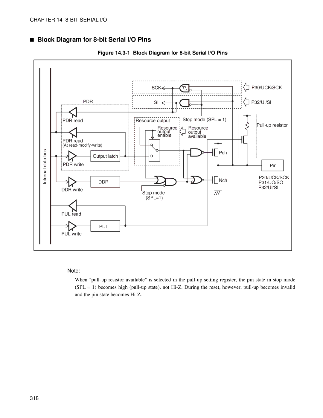
Chapter BIT Serial I/O
BIT Serial I/O
Serial Function Switching
Overview of 8-Bit Serial I/O
1 Shift Clock Cycle and Transfer Rate
Configuration of 8-Bit Serial I/O
1 Block Diagram of 8-bit Serial I/O
Shift clock counter
Serial mode register SMR
Shift clock control circuit
Bit serial I/O interrupt
P31/UO/SO pin
Pins of 8-Bit Serial I/O
P32/UI/SI pin
P30/UCK/SCK pin
Block Diagram for 8-bit Serial I/O Pins
318
Registers of 8-Bit Serial I/O
Bit Serial I/O Registers
Serial Mode Register SMR
2 Serial Mode Register SMR
CKS1, CKS0
Siof
Sioe
321
SST
BDS
322
Serial Data Register SDR
When the serial I/O is in transfer operation
Serial Data Register SDR
At serial output operation
Bit Serial I/O Interrupt Register and Vector Table
Interrupt of 8-Bit Serial I/O
1 8-bit Serial I/O Interrupt Register and Vector Table
Operations of Serial Output Functions
Serial output operation via internal shift clock
Operation at Serial Output Completion
Serial output operation using external shift clock
326
Serial input operation using internal shift clock
Operations of Serial Input Functions
Operation at Serial Input Completion
Serial input operation using external shift clock
328
Bit serial I/O operation in sleep mode
14.8 8-Bit Serial I/O Operation in Each Mode
Bit serial I/O operation in stop mode
330
When the External Shift Clock is Used
331
332
Malfunction due to noise
This section provides notes on using the 8-bit serial I/O
Error at serial transfer start
Shift clock idle state
Example of 8-Bit Serial I/O Connection
Bidirectional Serial I/O Operation
335
Program Example for 8-Bit Serial I/O
Pushw MOV
Program Example for 8-bit Serial Input
Wari Clrb Siof
Popw Reti Ends END
Pushw Xchw MOV SDR
338
Chapter Buzzer Output
1 Output Frequencies
Overview of the Buzzer Output
Buzzer Output
Clock supplier Buzzer output Square wave output at 12.5 MHz
Configuration of the Buzzer Output
Buzzer output selector
Pin of the Buzzer Output
Block Diagram of the Pin Related to the Buzzer Output
BZ pin
Buzzer Register Bzcr
1 Buzzer Register Bzcr
1 Functions of Each Bit in Buzzer Register Bzcr
344
Program Example for Buzzer Output
Bzcr EQU
346
Chapter Wild Register Function
Wild Register Function
Overview of the Wild Register Function
Wild Register Applicable Addresses
1 Wild Register Applicable Addresses
Memory area part
Configuration of the Wild Register Function
Control circuit part
Registers of the Wild Register Function
1 Registers Related to Wild Register Function
Wild register number Register name Function
Data Setting Registers WRDR0 and WRDR1
1 Functions of Data Setting Register Wrdr
WRDR0
WRARH0
Higher Address Set Registers WRARH0 and WRARH1
2 Functions of Higher Address Set Register Wrarh
WRARH1
WRARL0
Lower Address Set Registers WRARL0 and WRARL1
3 Functions of Lower Address Set Register Wrarl
WRARL1
Address Comparison EN Register Wren
5 Address Comparison EN Register Wren
Test register. Do not access this register
Data Test Set Register Wror
1 Operation Order of Wild Register
Operations of the Wild Register Functions
Wild Register Addresses List
2 Wild Register Addresses List
Chapter Flash Memory
Flash Memory Register
Overview of Flash Memory
Writing to/Erasing Flash Memory
Flash Memory
Flash Memory Control Status Register Fmcs
1 Flash Memory Control Status Register Fmcs
Inte
360
1 Command Sequence Table
Starting the Flash Memory Automatic Algorithm
2 Hardware Sequence Flag Functions
Confirming the Automatic Algorithm Execution State
1 Bit Assignments of Hardware Sequence Flags
State
Data Polling Flag DQ7
Automatic Erasing
Toggle Bit Flag DQ6
Timing Limit Exceeded Flag DQ5
Toggle Bit-2 Flag DQ2
Detailed Explanation of Writing to Erasing Flash Memory
Setting The Read/Reset State
Specifying Addresses
Writing Data
Writing to the Flash Memory
1 Example of the Flash Memory Write Procedure
370
Erasing All Data Erasing Chips
How to disable the Flash Security Feature
Flash Security Feature
How to enable the Flash Security Feature
Behavior under the Flash Security Feature
Program Access to Flash Memory
Software Reset, Watchdog Timer Reset
Flash Content Protection
374
Appendix
Appendix a I/O Map
Appendix a I/O Map
Table A-1 Map 1
Table A-1 Map 2
377
Table A-1 Map 3
378
Explanation on initial value
Table A-1 Map 4
Explanation on read/write
379
Appendix B Overview of the Instructions
Code Meaning
Explanation on the Codes Representing Instructions
Table B-1 Explanation on Codes on Instructions’ List
CCR
Table B-2 Explanation on Items of Instructions’ List
Explanation on the Items of Instructions’ List
382
Direct addressing
Addressing
Extended Addressing
Pointer Addressing
Index addressing
384
Vector Addressing
General-purpose Register Addressing
Immediate Addressing
Table B.1-1 Vector Table Address Corresponding to vct
Inherent addressing
Relative Addressing
386
JMP @A
Special Instructions
Movw A, PC
Divu a
Mulu a
388
Xchw A, PC
389
Appendix B Overview of the Instructions Callv #vct
390
Code Mnemonic
Bit Manipulation Instructions Setb and Clrb
Table B.3-1 Bus Operation at Bit Manipulation Instructions
RMW
F2MC-8L Instructions List
Table B.4-1 List of Transfer Instructions 1
Table B.4-1 List of Transfer Instructions 2
393
Table B.4-2 List of Operation Instructions 1
Operation Instructions
394
Table B.4-2 List of Operation Instructions 2
395
Table B.4-2 List of Operation Instructions 3
396
Table B.4-3 List Branch Instructions
Branch Instructions
Table B.4-2 List of Operation Instructions 4
397
Table B.4-4 List of Other Instructions
Other Instructions
398
Table B.5-1 shows the instruction map of the F2MC-8L
Instruction Map
Instruction Map
Instruction Map of the F
Appendix C Mask Options
Table C-1 Mask Options
Eprom for use
Appendix D Programming Eprom with Evaluation Chip
Programming Eprom
Appendix E Pin State of the MB89202/F202RA Series
Table E-1 Pin States in Each Operation Mode
Appendix E Pin State of the MB89202/F202RA Series
P37/BZ/PPG
Index follows on the next This is listed in alphabetic order
403
Numerics
ADC
Aden
CCR
Bzcr
Cntr
EIC
Comr
DDR
EIE
F2MC-8L
Fmcs
ILR
Interval Timer
Interrupt Enable Bits
Interrupt Level Setting Registers
Memory Access
OUT
P37/BZ/PPG
PDR
PUL
RCR
RST
Rsfr
SDR
SMR
Sidr
SMC
Sodr
TCR
Tbtc
Tccr
TDR
Wrarl
Wdtc
Wrarh
Wrdr
418
Fujitsu Semiconductor Controller Manual
CM25-10153-2E