MC68HC08KH12 Data Sheet
Page
Advance Information MC68HC708KH12
List of Sections
Page
Table of Contents
Random-Access Memory RAM
System Integration Module SIM
Clock Generator Module CGM
Universal Serial Bus Module USB
Monitor ROM MON
O Ports
Computer Operating Properly COP
Keyboard Interrupt Module KBI
Break Module Break
Mechanical Specifications
Page
Title
List of Figures
HDP1CR-HDP4CR
Title
Title
Title
List of Tables
Title
General Description
Contents
Introduction
Features
Page
1shows the structure of the MC68HC708KH12
MCU Block Diagram
MCU Block Diagram
2Shows the 64-pin QFP assignments
Pin Assignments
Power Supply Bypassing
SIM
Module KBI and . Timer Interface Module TIM.
Page
Memory Map
Memory Map
I/O Section
Control, Status, and Data Registers
Toie
Control, Status, and Data Registers
Pllie
Keyff
Rxdie
$FF8D $FFFF
Vector Addresses
Monitor ROM
1is a list of vector locations
Page
This section describes the 384 bytes of RAM
Random-Access Memory RAM
Functional Description
Page
Read-Only Memory ROM
Page
Configuration Register Config
= COP module disabled = COP module enabled
Configuration Register Config
Central Processor Unit CPU
CPU Registers
CPU Registers
Index Register HX
Stack Pointer SP
Program Counter PC
Condition Code Register CCR
Page
Arithmetic/Logic Unit ALU
Page
System Integration Module SIM
Introduction
SIM Block Diagram
SIM I/O Register Summary
SIM Bus Clock Control and Generation
1shows the internal signal names used in this section
Signal Name Conventions
Reset and System Initialization
PIN Bit Set Timing
External Reset Timing
Power-On Reset
COP reset is asynchronous to the bus clock
Computer Operating Properly COP Reset
POR Recovery
Universal Serial Bus Reset
Illegal Opcode Reset
Illegal Address Reset
SIM Counter
Exception Control
Interrupt Processing
Hardware Interrupts
Interrupt Entry
11.Interrupt Recognition Example
Interrupt Sources
SWI Instruction
12. Interrupt Status Register 1 INT1
Interrupt Status Register
14. Interrupt Status Register 2 INT2
13. Interrupt Status Register 2 INT2
Low-Power Modes
15. Wait Mode Entry Timing
16. Wait Recovery from Interrupt or Break
18. Stop Mode Entry Timing
SIM Registers
SIM Registers
21. Reset Status Register RSR
22. Break Flag Control Register Bfcr
Page
Clock Generator Module CGM
Introduction
1shows the structure of the CGM
CGM Block Diagram
Page
FRDV = fRCLK/R
Page
3MHz, or 1.5MHz respectively
Choose P = 0, 1, 2, or 3 for a bus frequency of 12MHz, 6MHz
CGM Numeric Example
Page
CGM External Connections
I/O Signals
Cgmvsel
CGM Registers
101
CGM I/O Register Summary
102
PLL Control Register Pctl
103
104
PRE10 Programming
105
PLL Multiplier Select Registers Pmshpmsl
RDS30 Reference Divider Select Bits
Initializes the register to $01 for a default divide value
Reference division factor R. See 8.4.3 PLL Circuits
Programming the PLL. RDS70 cannot be written when
107
Interrupts
Special Modes
108
Acquisition/Lock Time Specifications
109
110
111
112
113
Universal Serial Bus Module USB
114
115
Overview
116
I/O Register Description of the HUB function
117
HUB Control Register Summary
118
Setup
119
HUB Data Register Summary
120
USB HUB Root Port Control Register Hrpcr
121
USB HUB Downstream Port Control Registers
122
123
USB SIE Timing Interrupt Register Sietir
124
125
USB SIE Timing Status Register Sietsr
126
127
USB HUB Address Register Haddr
128
USB HUB Interrupt Register 0 HIR0
129
USB HUB Control Register 0 HCR0
130
131
USB HUB Control Register 1 HCR1
132
10. USB HUB Status Register HSR
133
134
I/O Register Description of the Embedded Device Function
135
Embedded Device Control Register Summary
136
Embedded Device Data Register Summary
DE1D0
137
13. USB Embedded Device Interrupt Register 0 DIR0
12. USB Embedded Device Address Register Daddr
139
140
14. USB Embedded Device Interrupt Register 1 DIR1
141
15. USB Embedded Device Control Register 0 DCR0
142
143
16. USB Embedded Device Control Register 1 DCR1
144
17. USB Embedded Device Status Register DSR
145
146
18. USB Embedded Device Control Register 2 DCR2
147
19. USB Embedded Device Endpoint 0 Data Register UE0D0-UE0D7
148
20. USB Embedded Device Endpoint 0 Data Register UE0D0-UE0D7
149
Monitor ROM MON
150
151
Monitor Mode Circuit
152
Mode Selection
153
Mode Differences
Sample Monitor Waveforms
Monitor Data Format
155
Break Transaction
156
Read Read Memory Command
Write Write Memory Command
157
Iread Indexed Read Command
Iwrite Indexed Write Command
158
Readsp Read Stack Pointer Command
RUN Run User Program Command
159
Monitor Baud Rate Selection
160
161
Timer Interface Module TIM
162
163
TIM Block Diagram
164
TIM I/O Register Summary
165
Buffered Output Compare
Unbuffered Output Compare
Registers of the linked pair alternately control the output
166
167
168
Unbuffered PWM Signal Generation
169
Buffered PWM Signal Generation
170
PWM Initialization
TIM status control register TSC, clear the TIM stop bit
171
Wait Mode
172
11.8 I/O Signals
TIM During Break Interrupts
Minimum Tclk pulse width, Tclklmin or TCLKHMIN, is
11.9 I/O Registers
Maximum Tclk frequency is
173
174
Resets the TIM counter Prescales the TIM counter clock
175
Prescaler Selection
176
TIM Counter Registers Tcnthtcntl
177
TIM Counter Modulo Registers Tmodhtmodl
178
TIM Channel Status and Control Registers TSC0TSC1
179
See Table
180
Mode, Edge, and Level Selection
181
CHxMAX Latency
182
TIM Channel Registers TCH0H/LTCH1H/L
183
O Ports
184
I/O Port Register Summary
$0007 $0008 $0009 $000A $000B $001C $001D
185
186
Port a
3shows the port a I/O logic
Data Direction Register a Ddra
188
Port B
Port a Pin Functions
6shows the port B I/O logic
Data Direction Register B Ddrb
190
Port C
Port B Pin Functions
191
Data Direction Register C Ddrc
192
Port D
Port C Pin Functions
193
10. Port D Data Register PTD
12shows the port D I/O logic
11. Data Direction Register D Ddrd
195
Port E
Port D Pin Functions
196
KBI
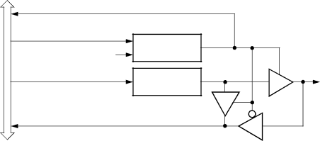
15shows the port E I/O logic
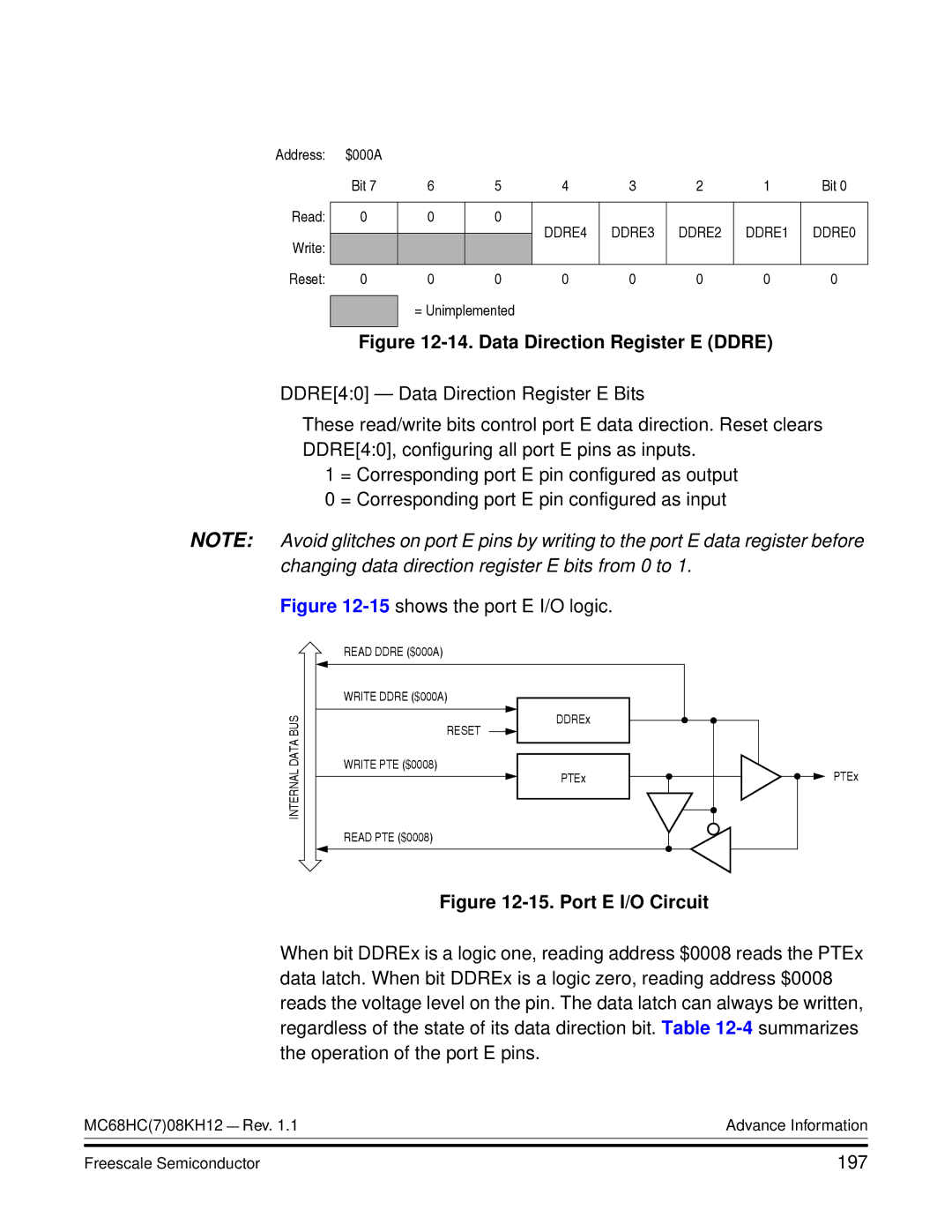
14. Data Direction Register E Ddre
198
Port E Pin Functions
PTE0-PTE1 / PTE2-PTE3
199
200
17. Optical Interface Voltage References
201
18. Port E Optical Coupling Interface
202
Port F
3shows the port F I/O logic
20. Data Direction Register F Ddrf
204
Port Options
Port F Pin Functions
205
206
207
Computer Operating Properly COP
1shows the structure of the COP module
COP Block Diagram COP I/O Port Register Summary
209
13.4 I/O Signals
210
COP Control Register Copctl
Monitor Mode
COP does not generate CPU interrupt requests
211
212
COP Module During Break Mode
213
External Interrupt IRQ
IRQ module provides a non-maskable interrupt input
214
215
IRQ Module Block Diagram IRQ I/O Port Register Summary
216
217
IRQ Module During Break Interrupts
IRQ Status and Control Register Iscr
218
219
Keyboard Interrupt Module KBI
220
221
KBI I/O Register Summary
222
Port-D Keyboard Interrupt Block Diagram
223
224
225
Port-D Keyboard Status and Control Register
226
Port-D Keyboard Interrupt Enable Register
227
228
Port-E Keyboard Interrupt Block Diagram
229
$FFED
230
231
Port-E Keyboard Status and Control Register
232
Port-E Keyboard Interrupt Enable Register
233
234
Port-F Keyboard Interrupt Block Diagram
235
236
237
Port-F Keyboard Status and Control Register
238
Port-F Keyboard Interrupt Enable Register
Port-F Pull-up Enable Register
Stop Mode
Keyboard Module During Break Interrupts
239
240
241
Break Module Break
242
243
Break Module Block Diagram Break I/O Register Summary
244
Break Module Registers
245
Break Status and Control Register Brkscr
246
Break Address Registers Brkh and Brkl
247
Preliminary Electrical Specifications
248
Absolute Maximum Ratings
249
Thermal Characteristics
Functional Operating Range
250
DC Electrical Characteristics
251
Oscillator Characteristics
Control Timing
252
USB DC Electrical Characteristics
253
USB Low Speed Source Electrical Characteristics
254
USB High Speed Source Electrical Characteristics
255
HUB Repeater Electrical Characteristics
256
USB Signaling Levels
TImer Interface Module Characteristics
257
Clock Generation Module Characteristics
258
Acquisition/Lock Time Specifications
259
Mechanical Specifications
260
Plastic Quad Flat Pack QFP
Page
How to Reach Us