Chapter 5 Input/Output Interfaces
5.7.2 USB PROGRAMMING
Programming the USB interface consists of configuration, which typically occurs during POST, and control, which occurs at runtime.
5.7.2.1 USB Configuration
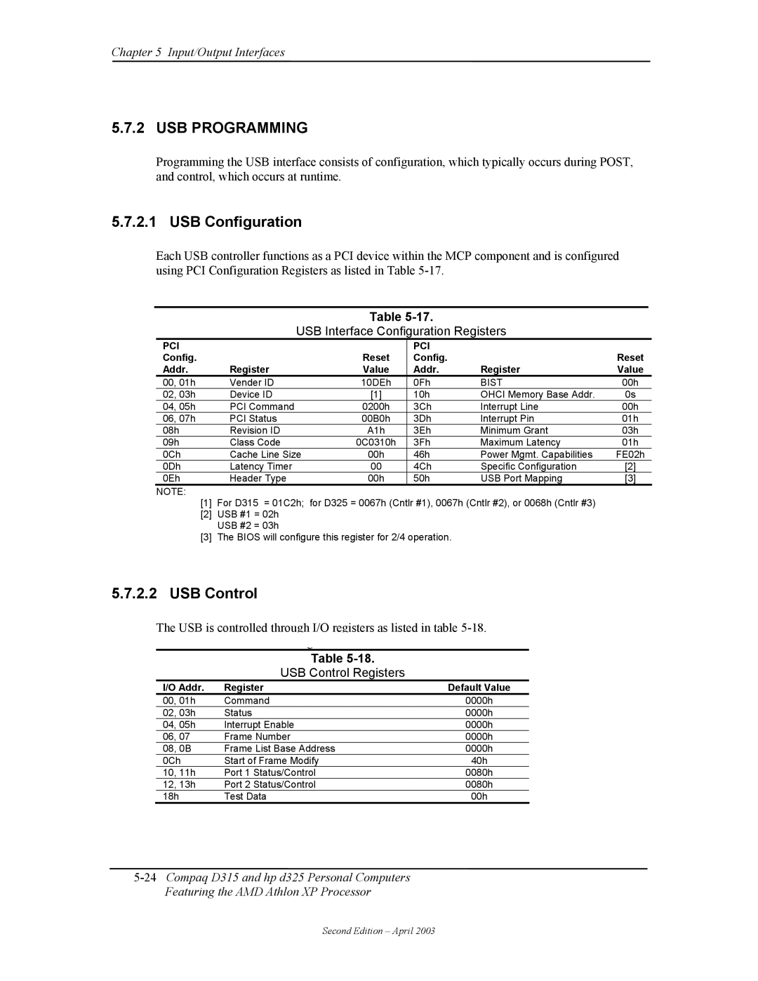
Each USB controller functions as a PCI device within the MCP component and is configured using PCI Configuration Registers as listed in Table
Table
Table
USB Interface Configuration Registers
PCI |
|
| PCI |
|
|
Config. |
| Reset | Config. |
| Reset |
Addr. | Register | Value | Addr. | Register | Value |
00, 01h | Vender ID | 10DEh | 0Fh | BIST | 00h |
02, 03h | Device ID | [1] | 10h | OHCI Memory Base Addr. | 0s |
04, 05h | PCI Command | 0200h | 3Ch | Interrupt Line | 00h |
06, 07h | PCI Status | 00B0h | 3Dh | Interrupt Pin | 01h |
08h | Revision ID | A1h | 3Eh | Minimum Grant | 03h |
09h | Class Code | 0C0310h | 3Fh | Maximum Latency | 01h |
0Ch | Cache Line Size | 00h | 46h | Power Mgmt. Capabilities | FE02h |
0Dh | Latency Timer | 00 | 4Ch | Specific Configuration | [2] |
0Eh | Header Type | 00h | 50h | USB Port Mapping | [3] |
NOTE:
[1]For D315 = 01C2h; for D325 = 0067h (Cntlr #1), 0067h (Cntlr #2), or 0068h (Cntlr #3)
[2]USB #1 = 02h USB #2 = 03h
[3]The BIOS will configure this register for 2/4 operation.
5.7.2.2USB Control
The USB is controlled through I/O registers as listed in table
Table
Table
USB Control Registers
I/O Addr. | Register | Default Value |
00, 01h | Command | 0000h |
02, 03h | Status | 0000h |
04, 05h | Interrupt Enable | 0000h |
06, 07 | Frame Number | 0000h |
08, 0B | Frame List Base Address | 0000h |
0Ch | Start of Frame Modify | 40h |
10, 11h | Port 1 Status/Control | 0080h |
12, 13h | Port 2 Status/Control | 0080h |
18h | Test Data | 00h |
Second Edition – April 2003
