Technical Reference Guide

4.2.1 PCI BUS TRANSACTIONS

The PCI bus consists of a 32-bit path (AD31-00 lines) that uses a multiplexed scheme for handling both address and data transfers. A bus transaction consists of an address cycle and one or more data cycles, with each cycle requiring a clock (PCICLK) cycle. High performance is realized during burst modes in which a transaction with contiguous memory locations requires that only one address cycle be conducted and subsequent data cycles are completed using auto- incremented addressing. Four types of address cycles can take place on the PCI bus; I/O, memory, configuration, and special. Address decoding is distributed (left up to each device on the PCI bus).

4.2.1.1I/O and Memory Cycles

For I/O and memory cycles, a standard 32-bit address decode (AD31..0) for byte-level addressing is handled by the appropriate PCI device. For memory addressing, PCI devices decode the AD31..2 lines for dword-level addressing and check the AD1,0 lines for burst (linear- incrementing) mode. In burst mode, subsequent data phases are conducted a dword at a time with addressing assumed to increment accordingly (four bytes at a time).

4.2.1.2Configuration Cycles

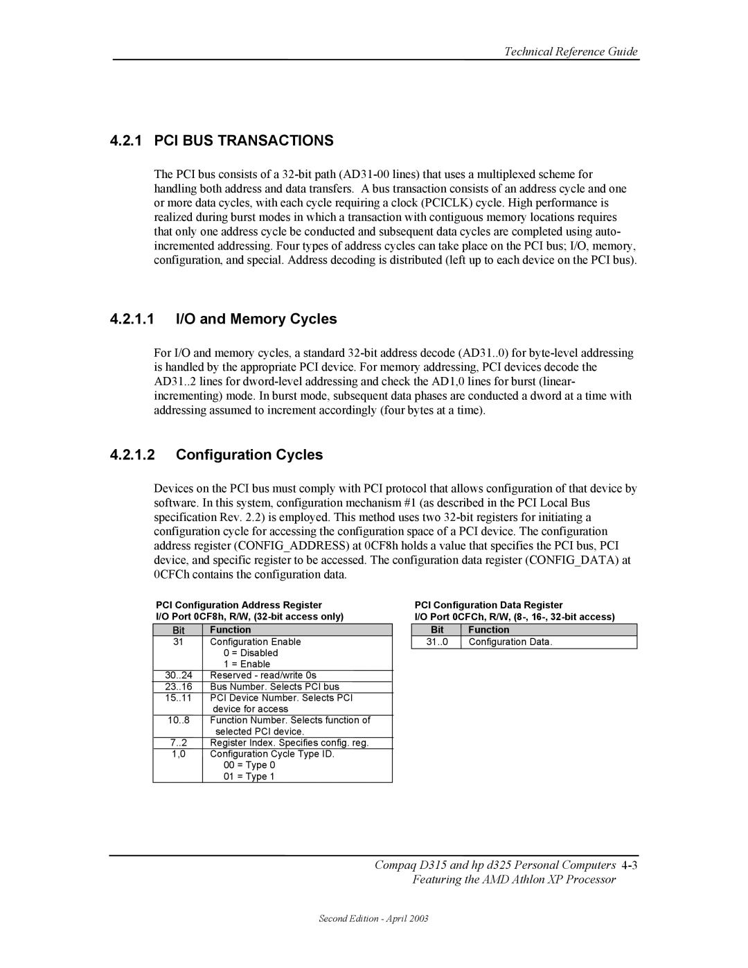
Devices on the PCI bus must comply with PCI protocol that allows configuration of that device by software. In this system, configuration mechanism #1 (as described in the PCI Local Bus specification Rev. 2.2) is employed. This method uses two 32-bit registers for initiating a configuration cycle for accessing the configuration space of a PCI device. The configuration address register (CONFIG_ADDRESS) at 0CF8h holds a value that specifies the PCI bus, PCI device, and specific register to be accessed. The configuration data register (CONFIG_DATA) at 0CFCh contains the configuration data.

PCI Configuration Address Register

I/O Port 0CF8h, R/W, (32-bit access only)

Bit

Function

31

Configuration Enable


0 = Disabled


1 = Enable

30..24

Reserved - read/write 0s

23..16

Bus Number. Selects PCI bus

15..11

PCI Device Number. Selects PCI


device for access

10..8

Function Number. Selects function of


selected PCI device.

7..2

Register Index. Specifies config. reg.

1,0

Configuration Cycle Type ID.


00 = Type 0


01 = Type 1

PCI Configuration Data Register

I/O Port 0CFCh, R/W, (8-, 16-, 32-bit access)

Bit Function

31..0 Configuration Data.

Compaq D315 and hp d325 Personal Computers 4-3Featuring the AMD Athlon XP Processor

Second Edition - April 2003

Page 53
Image 53
HP D315 manual PCI BUS Transactions, 1.1 I/O and Memory Cycles, Configuration Cycles