1 |
Hardware Preparation and Installation
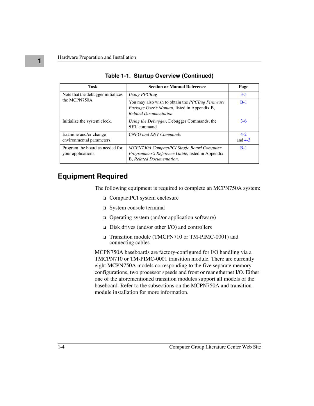
Table 1-1. Startup Overview (Continued)
Task | Section or Manual Reference | Page | |
|
|
| |
Note that the debugger initializes | Using PPCBug | ||
the MCPN750A |
|
| |
You may also wish to obtain the PPCBug Firmware | |||
| |||
| Package User’s Manual, listed in Appendix B, |
| |
| Related Documentation. |
| |
|
|
| |
Initialize the system clock. | Using the Debugger, Debugger Commands, the | ||
| SET command |
| |
|
|
| |
Examine and/or change | CNFG and ENV Commands | ||
environmental parameters. |
| and | |
|
|
| |
Program the board as needed for | MCPN750A CompactPCI Single Board Computer | ||
your applications. | Programmer’s Reference Guide , listed in Appendix |
| |
| B, Related Documentation. |
| |
|
|
|
Equipment Required
The following equipment is required to complete an MCPN750A system:
❏CompactPCI system enclosure
❏System console terminal
❏Operating system (and/or application software)
❏Disk drives (and/or other I/O) and controllers
❏Transition module (TMCPN710 or
MCPN750A baseboards are
Computer Group Literature Center Web Site |