2 |
Startup and Operation
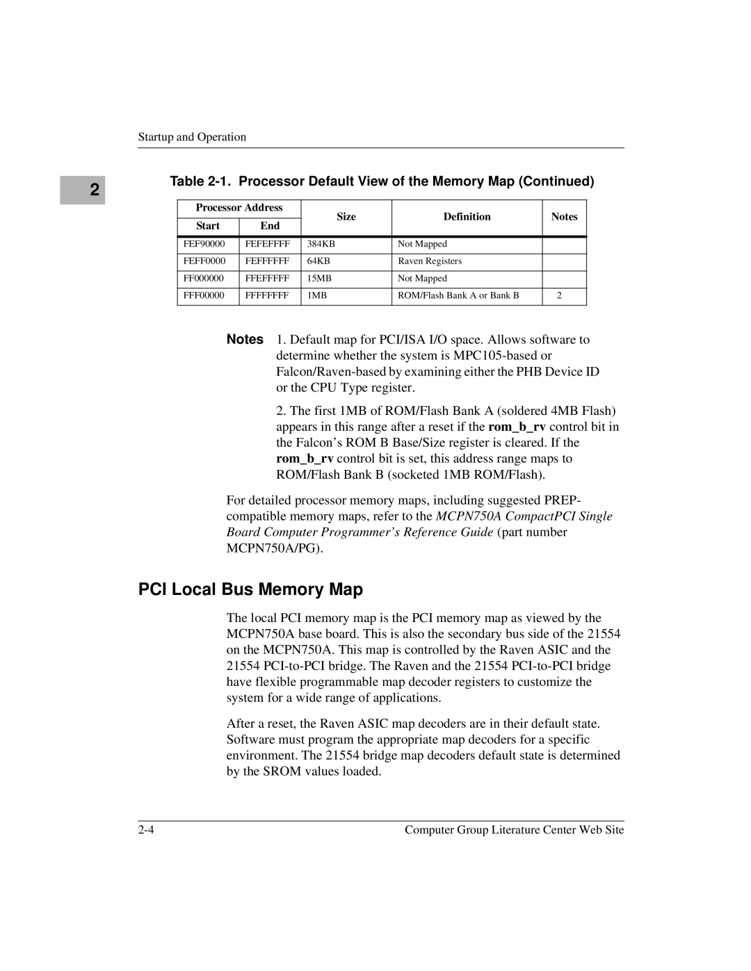
Table 2-1. Processor Default View of the Memory Map (Continued)
Processor Address | Size | Definition | Notes | |
|
| |||
Start | End |
|
|
|
|
|
|
|
|
FEF90000 | FEFEFFFF | 384KB | Not Mapped |
|
|
|
|
|
|
FEFF0000 | FEFFFFFF | 64KB | Raven Registers |
|
|
|
|
|
|
FF000000 | FFEFFFFF | 15MB | Not Mapped |
|
|
|
|
|
|
FFF00000 | FFFFFFFF | 1MB | ROM/Flash Bank A or Bank B | 2 |
|
|
|
|
|
Notes 1. Default map for PCI/ISA I/O space. Allows software to determine whether the system is
2.The first 1MB of ROM/Flash Bank A (soldered 4MB Flash) appears in this range after a reset if the rom_b_rv control bit in the Falcon’s ROM B Base/Size register is cleared. If the rom_b_rv control bit is set, this address range maps to ROM/Flash Bank B (socketed 1MB ROM/Flash).
For detailed processor memory maps, including suggested PREP- compatible memory maps, refer to the MCPN750A CompactPCI Single Board Computer Programmer’s Reference Guide (part number MCPN750A/PG).
PCI Local Bus Memory Map
The local PCI memory map is the PCI memory map as viewed by the MCPN750A base board. This is also the secondary bus side of the 21554 on the MCPN750A. This map is controlled by the Raven ASIC and the 21554
After a reset, the Raven ASIC map decoders are in their default state. Software must program the appropriate map decoders for a specific environment. The 21554 bridge map decoders default state is determined by the SROM values loaded.
Computer Group Literature Center Web Site |
