Preparation
The MCPN750A is factory tested and shipped with the configurations described in the following sections. The MCPN750A’s required and
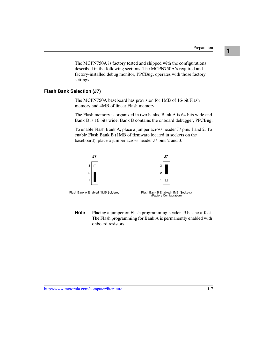
Flash Bank Selection (J7)
The MCPN750A baseboard has provision for 1MB of
The Flash memory is organized in two banks, Bank A is 64 bits wide and Bank B is 16 bits wide. Bank B contains the onboard debugger, PPCBug.
To enable Flash Bank A, place a jumper across header J7 pins 1 and 2. To enable Flash Bank B (1MB of firmware located in sockets on the baseboard), place a jumper across header J7 pins 2 and 3.
| J7 |
| J7 | ||||||
3 |
|
|
|
| 3 |
|
|
|
|
|
|
|
|
|
|
|
| ||
|
|
|
|
|
|
| |||
2 |
|
|
|
| 2 |
|
|
|
|
|
|
|
| ||||||
1 |
|
|
|
| 1 |
|
|
|
|
|
|
|
|
|
|
|
|
|
|
Flash Bank A Enabled (4MB Soldered) | Flash Bank B Enabled (1MB, Sockets) | ||||||||
|
|
|
|
| (Factory Configuration) | ||||
Note Placing a jumper on Flash programming header J9 has no affect. The Flash programming for Bank A is permanently enabled with onboard resistors.
1 |
http://www.motorola.com/computer/literature |