Introduction
Command/response Register Description
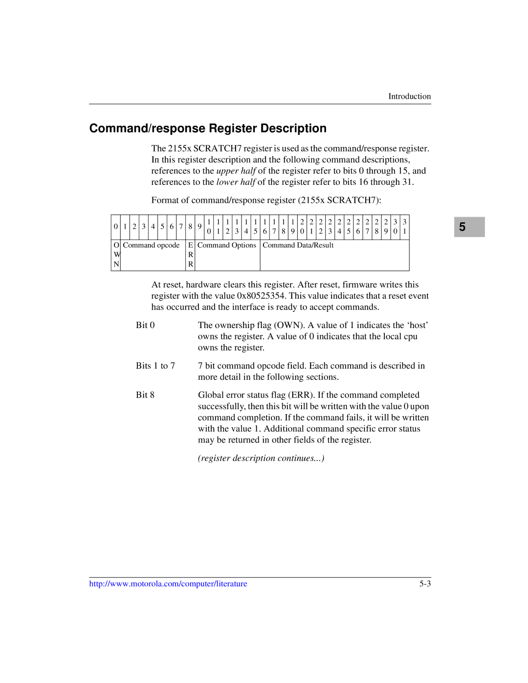
The 2155x SCRATCH7 register is used as the command/response register. In this register description and the following command descriptions, references to the upper half of the register refer to bits 0 through 15, and references to the lower half of the register refer to bits 16 through 31.
Format of command/response register (2155x SCRATCH7):
0 | 1 | 2 | 3 | 4 | 5 | 6 | 7 | 8 | 9 | 1 | 1 | 1 | 1 | 1 | 1 | 1 | 1 | 1 | 1 | 2 | 2 | 2 | 2 | 2 | 2 | 2 | 2 | 2 | 2 | 3 | 3 |
|
|
|
|
|
|
|
|
|
| 0 | 1 | 2 | 3 | 4 | 5 | 6 | 7 | 8 | 9 | 0 | 1 | 2 | 3 | 4 | 5 | 6 | 7 | 8 | 9 | 0 | 1 |
|
|
|
|
|
|
|
|
|
|
|
|
|
|
|
|
|
|
|
|
|
|
|
|
|
|
|
|
|
|
|
|
O | Command opcode | E | Command Options | Command Data/Result |
|
|
|
|
|
|
|
| |||||||||||||||||||
W |
|
|
|
|
|
|
| R |
|
|
|
|
|
|
|
|
|
|
|
|
|
|
|
|
|
|
|
|
|
|
|
N |
|
|
|
|
|
|
| R |
|
|
|
|
|
|
|
|
|
|
|
|
|
|
|
|
|
|
|
|
|
|
|
|
|
|
|
|
|
|
|
|
|
|
|
|
|
|
|
|
|
|
|
|
|
|
|
|
|
|
|
|
|
|
|
At reset, hardware clears this register. After reset, firmware writes this register with the value 0x80525354. This value indicates that a reset event has occurred and the interface is ready to accept commands.
Bit 0 | The ownership flag (OWN). A value of 1 indicates the ‘host’ |
| owns the register. A value of 0 indicates that the local cpu |
| owns the register. |
Bits 1 to 7 | 7 bit command opcode field. Each command is described in |
| more detail in the following sections. |
Bit 8 | Global error status flag (ERR). If the command completed |
| successfully, then this bit will be written with the value 0 upon |
| command completion. If the command fails, it will be written |
| with the value 1. Additional command specific error status |
| may be returned in other fields of the register. |
| (register description continues...) |
5 |
http://www.motorola.com/computer/literature |
