DATASHEET
PM5349 S/UNI-QUAD
ISSUE 6 | SATURN USER NETWORK INTERFACE | |
|
|
|
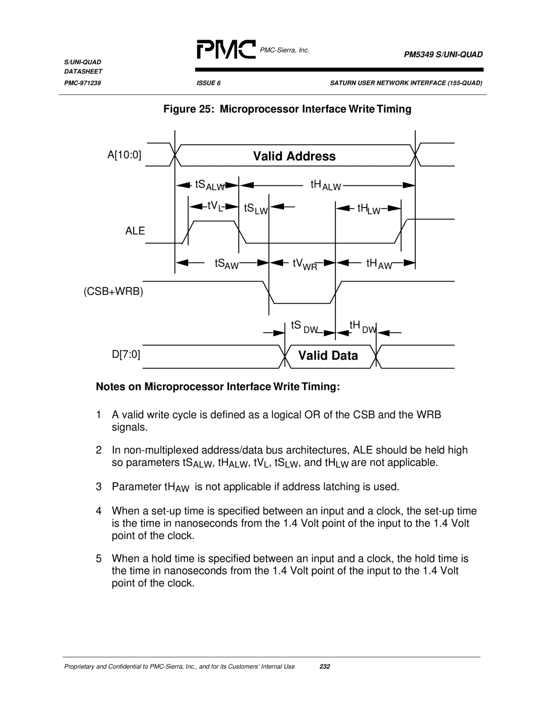
Figure 25: Microprocessor Interface Write Timing
A[10:0]
ALE
(CSB+WRB)
D[7:0]
Valid Address
 tSALW
tSALW
 tHALW
tHALW
tVL | tS | LW |
|
|
| tH |
| ||||||
|
|
| ||||
|
|
|
|
| LW |
tSAW 

 tVWR
tVWR 
 tHAW
tHAW

tS DW |
|
|
| tH DW |
Valid Data
Notes on Microprocessor Interface Write Timing:
1A valid write cycle is defined as a logical OR of the CSB and the WRB signals.
2In
3Parameter tHAW is not applicable if address latching is used.
4When a
5When a hold time is specified between an input and a clock, the hold time is the time in nanoseconds from the 1.4 Volt point of the input to the 1.4 Volt point of the clock.
Proprietary and Confidential to | 232 |