DATASHEET
PM5349 S/UNI-QUAD
ISSUE 6 | SATURN USER NETWORK INTERFACE | |
|
|
|
otherwise be coupled into the analog circuitry. Current limiting can be accomplished by using an off chip three terminal voltage regulator supplied by a quiet high voltage supply. If the VDD power supply is relatively quiet, VDD can be filtered using a ferrite bead and a high frequency decoupling capacitor to supply AVD. The relative power sequencing of the multiple AVD power supplies is not important.
5.) Power down the device in the reverse sequence. Use the above current limiting technique for the analog power supplies. Small offsets in VDD / AVD discharge times will not damage the device.
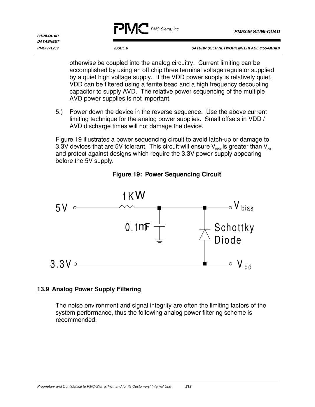
Figure 19 illustrates a power sequencing circuit to avoid latch-up or damage to
3.3V devices that are 5V tolerant. This circuit will ensure Vbias is greater than Vdd and protect against designs which require the 3.3V power supply appearing
before the 5V supply.
Figure 19: Power Sequencing Circuit
1 K Ω
5 V
0 . 1μF
3 . 3 V
V b i a s
S c h o t t k y D i o d e
V d d
13.9 Analog Power Supply Filtering
The noise environment and signal integrity are often the limiting factors of the system performance, thus the following analog power filtering scheme is recommended.
Proprietary and Confidential to | 219 |