Page
Errata VER
Features
Low Voltage Reset
Built-in Reset circuit LVR
VDD
Reset
BGR
Parameter Symbol Conditions Min Typ Max Unit
D.C. Electrical Characteristics
Pull-up resistor
VDD = 4.5V to RUN mode MHz CPU clock VDD = Vlvr to 5.5
Sub Oscillator Frequency
A.C. Electrical Characteristics
Main Oscillator Frequency
Main Oscillator Clock Stabilization TimePAGE
Oscillator Test Condition Min Typ Max Unit
Data Retention Supply Voltage in Stop Mode
10. Uart Timing Characteristics in Mode 0
Parameter Symbol Min Typ Max Unit
Operating Voltage RangePAGE
11. A/D Converter Electrical Characteristics
12. LVR Low Voltage Reset Circuit Characteristics
Comparison of S3P84E9 and S3C84E5/C84E9 Features
S3C84E5/C84E9/P84E9
Important Notice
Uart
Part Programming Model
Iii
Table of Contents
Overview
Chapter Interrupt Structure
Vii
Part II Hardware Descriptions
Viii
Chapter
HEX2ROM
Title Number
List of Figures
Xii
10-2
10-4
11-8
13-7
12-4
12-5
13-3
17-11
17-2
Xvi
Chapter Converter Configuring A/D Converter 15-6
Chapter Bit Timer A/B
Chapter Bit Timer 10,1
Chapter Watch Timer
Register Full Register Name Identifier Number
Instruction Full Register Name Mnemonic Number
LDCPD/LDEPD
LDC/LDE
LDCD/LDED
LDCI/LDEI
S3C8-SERIES Microcontrollers
Product Overview
S3C84E5/C84E9/P84E9 Microcontroller
CPU
Features
S3C84E5/C84E9/P84E9 Block Diagram
Block Diagram
44-QFP
NRESET
PIN Assignment
Top View
Sdip
S3C84E5
S3C84E9
S3P84E9
PIN Descriptions
Type Description Number Pins
S3C84E5/C84E9/P84E9 Pin Descriptions Circuit Share
Test
INT0-INT10
AVREF, Avss
BUZ
PIN Circuits
Pin Circuit Type B nRESET
Pin Circuit Type D P0.2-P0.7, P1, P4.3-P4.5
Pin Circuit Type E P3
Overview
Address Spaces
HEX
Program Memory ROM
0FFH
590
Register Architecture
S3C84E5/C84E9/P84E9 Register Type Summary Number of Bytes
Total Addressable Bytes
Page01 PagePage00 Set
Set1 Bank
MSB LSB
Register page Pointer PP
RAMCL1 CLR
SRP
RAMCL0 CLR
Djnz R0,RAMCL0 CLR
Register SET
C0H BFH
Prime Register Space
FFH F0H E0H D0H C0H
Set Bank
F8H
Working Registers
F7H
SRP0
Using the Register Pointers
Programming TIP Setting the Register Pointers
SRP1
+ R2 + C
#80H RP0 ← 80H
R0,R1 ← R0 + R1
R0,R2
Bit Register Pair
Register Addressing
Prime Registers
FFH E0H D0H C0H BFH
Control Registers System
Register Pointers
E0H D0H C0H BFH
Common Working Register Area C0H-CFH
RP1 → C8H-CFH
FFH F0H
BIT Working Register Addressing
Programming TIP Addressing the Common Working Register Area
Examples
Example
R6 Opcode
RP0 RP1
13 -Bit Working Register Addressing
14 -Bit Working Register Addressing Example
High Address
System and User Stack
Stack Operations
Stack Pointers SPL, SPH
POP RP1
SPL,#0FFH SPL ← FFH
Push RP0
Push RP1
Addressing Modes
Operand
Register Addressing Mode R
Opcode
DEC Cntr
Address
Indirect Register Addressing Mode IR
@SHIFT
Register Pair
Indirect Register Addressing Mode
Call @RR2 JP @RR2
Indirect Working Register Addressing to Register File
LDE
LCD
Index
Indexed Addressing Mode
Offset
Indexed Addressing Mode
LDC
Indexed Addressing to Program or Data Memory
10. Direct Addressing for Load Instructions
Direct Address Mode DA
JOB1
Direct Address Mode
Call Display
Call #40H
Indirect Address Mode IA
ULT,$+OFFSET
Relative Address Mode RA
Operand Opcode
Immediate Mode IM
LD R0,#0AAH
Set 1 Registers Register Name Mnemonic Decimal Hex
Control Registers
Set 1, Bank 0 Registers Register Name Mnemonic Decimal Hex
Set 1, Bank 1 Registers Register Name Mnemonic Decimal Hex
Sign Flag S
Bit Identifier Reset Value Read/Write Bit Addressing
Mode Carry Flag C
Zero Flag Z
Adcon A/D Converter Control Register F7H Set 1, Bank
D3H
Btcon Basic Timer Control Register
Fxx/2
Clkcon System Clock Control Register
D4H
CPU Clock System Clock Selection Bits note
D5H
Flags System Flags Register
DDH
IMR Interrupt Mask Register
DBH
IPH Instruction Pointer High Byte
DAH
IPL Instruction Pointer Low Byte
FFH
IPR Interrupt Priority Register
DCH
IRQ Interrupt Request Register
Sub System Oscillator Control Bit
Osccon Oscillator Control Register FBH Set 1, Bank
Sub-system Oscillator Driving Ability Control Bit
Main System Oscillator Control Bit
P0.4/T1OUT1 Configuration Bits
P0.7/TACAP Configuration Bits
P0.6/TACK Configuration Bits
P0.5/T1CAP0 Configuration Bits
P0.0/XTin Configuration Bits
P0.3/T1CK1 Configuration Bits
P0.2/T1CAP1 Configuration Bits
P0.1/XTout Configuration Bits
P1.4/RXD Configuration Bits
P1.5/TXD Configuration Bits
P1CONH Port 1 Control Register High Byte E8H Set 1, Bank
P1.0/TAOUT Configuration Bits
P1.3/BZOUT Configuration Bits
P1.2/T1OUT0 Configuration Bits
P1.1/T1CK0 Configuration Bits
P2.5/ INT5
P2CONH Port 2 Control Register High Byte EAH Set 1, Bank
P2.7/INT7
P2.6/ INT6
P2.1/INT1
P2CONL Port 2 Control Register Low Byte EBH Set 1, Bank
P2.3/INT3
P2.2/INT2
ECH
P2INT Port 2 Interrupt Control Register
EDH
P2INTPND Port 2 Interrupt Pending Register
2P3.5/ADC5
P3CONH Port 3 Control Register High Byte EEH Set 1, Bank
P3.7/ADC7
4P3.6/ADC6
3P3.1/ADC1
P3CONL Port 3 Control Register Low Byte EFH Set 1, Bank
P3.3/ADC3
4P3.2/ADC2
P4.4
Input mode Push-pull output mode
P4CONH Port 4 Control Register High Byte F0H Set 1, Bank
P4.5
P4.1/INT9
P4CONL Port 4 Control Register Low Byte F1H Set 1, Bank
P4.3/TBPWM
P4.2/INT10
P4INT Port 4 Interrupt Control Register
P4.2 External Interrupt INT10 Enable Bit
P4.1 External Interrupt INT9 Enable Bit
P4.0 External Interrupt INT8 Enable Bit
P4.1/PND9 Interrupt Pending Bit
P4INTPND Port 4 Interrupt Pending Register
F3H
P4.2/PND10 Interrupt Pending Bit
Source Register Page Selection Bits
PP Register Page Pointer
DFH
Destination Register Page Selection Bits
D7H
RP0 Register Pointer
D6H
RP1 Register Pointer
SPL Stack Pointer Low Byte
SPH Stack Pointer High Byte
D8H
Set
Stop Control Bits
Stpcon Stop Control Register E5H Set 1, Bank
DEH
SYM System Mode Register
Fast Interrupt Enable Bit
Global Interrupt Enable Bit note
T1CON0 Timer 10 Control Register E8H Set 1, Bank
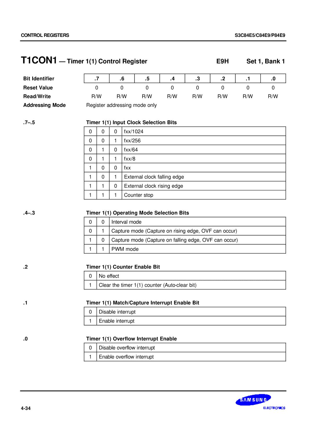
T1CON1 Timer 11 Control Register E9H Set 1, Bank
Tacon Timer a Control Register E1H Set 1, Bank
D0H
Tbcon Timer B Control Register
Tintpnd Timer A, Timer 1 Interrupt Pending Register E0H
Transmit Interrupt Enable Bit
Multiprocessor Communication 1 Enable Bit for mode 2 only
Serial Data Receive Enable Bit
Receive Interrupt Enable Bit
Control Register
Uartpnd Uart Pending and parity control F4H Set 1, Bank
Wtcon Watch Timer Control Register FAH Set 1, Bank
Sources
Interrupt Structure
Levels
Vectors
Levels Type 1 IRQn Type 2 IRQn Type 3 IRQn Vectors Sources
Interrupt Types
S3C84E5/C84E9/P84E9 Interrupt Structure
Levels
Vectors Sources ResetClear
Interrupt Vector Area
Interrupt Vector Addresses
HEX 7FFFH 3FFFH
Level
SYSTEM-LEVEL Interrupt Control Registers
ENABLE/DISABLE Interrupt Instructions EI, DI
Interrupt Control Register Overview Function Description
Interrupt Processing Control Points
Interrupt Function Diagram
Peripheral Interrupt Control Registers
IRQ0
System Mode Register SYM
IRQ1 IRQ2 IRQ3 IRQ4 IRQ5 IRQ6 IRQ7
MSB
Interrupt Mask Register IMR
LSB IRQ1 IRQ0 IRQ7 IRQ6 IRQ5 IRQ4 IRQ3 IRQ2
Group B IRQ2, IRQ3, IRQ4 Group C IRQ5, IRQ6, IRQ7
Interrupt Priority Register IPR
Group a
IRQ0, IRQ1
Interrupt Priority Register IPR
Interrupt Request Register IRQ
Interrupt Request Register IRQ
Pending Bits Cleared Automatically by Hardware
Pending Bits Cleared by the Service Routine
Interrupt Pending Function Types
Overview
Interrupt Source Polling Sequence
Interrupt Service Routines
Nesting of Vectored Interrupts
Generating Interrupt Vector Addresses
Addressing Modes
Instruction SET
Data Types
Register Addressing
Ldcd
LDE
LDC
Lded
Logic Instructions
Bit Manipulation Instructions
CPU Control Instructions
System Flags Register Flags
Flags Register Flags
Flag Descriptions
Flag Notation Conventions
Instruction Set Symbols
Symbol Description
Instruction SET Notation
IRR
Immediate long addressing mode #data Data =
IML
Opcode MAP Lower Nibble HEX
Opcode Quick Reference
Idle
Djnz INC Next
R1,R2 R2,R1
Djnz INC NOP
Condition Codes Binary Mnemonic Description Flags Set
Condition Codes
Instruction Descriptions
ADC
ADC Add with Carry
Bytes Cycles Opcode
ADD Add
ADD
Format
Logical
R1,01H.1 R1 = 06H, register 01H = 05H
Band Bit
Src Opc
Given R1 = 07H and register 01H = 05H
BCP
BCP Bit Compare
Bitc
Bitc Bit Complement
Hex Dst
BITRdst.b Operation dstb ←
Bitr Bit Reset
BITSdst.b Operation dstb ←
Bits Bit Set
BOR
BOR Bit or
Btjrf SKIP,R1.3
Btjrf Bit Test, Jump Relative on False
PC jumps to Skip location
Btjrt SKIP,R1.1
Btjrt Bit Test, Jump Relative on True
Btjrt
If srcb is a 1, then PC ← PC + dst
R1,01H.1 R1 = 06H, register 01H 03H
Bxor Bit XOR
@SP ← PCH
Call Call Procedure
Call dst Operation SP ← SP-1
@SP ← PCL
Format Bytes Cycles Opcode Hex
CCF Complement Carry Flag
CCF
Operation C ← not C
CLRdst Operation dst ←
CLR Clear
00H Register 00H
0F8H
COM Complement
COMdst Operation dst ← not dst
Opc Dst Examples Given R1 = 07H and register 07H = 0F1H
UGE,SKIP INC Skip
Format Bytes Cycles Opcode Addr Mode Hex Dst Src
CP Compare
Operation dst-src
If dst-src = 0, PC
Cpije Compare, Increment, and Jump on Equal
Cpije
Dst,src,RA
Example Given R1 = 02H, R2 = 03H, and register 03H = 04H
Cpijne Compare, Increment, and Jump on Non-Equal
Cpijne
Opc Src Dst
ADD ADC
DA Decimal Adjust
DAdst Operation dst ← DA dst
After DA
3CH
Opc Dst Examples Given R1 = 03H and register 03H = 10H
Contents of the destination operand are decremented by one
DEC Decrement
DECdst Operation dst ← dst-1
Loop Decw RR0
Decw Decrement Word
Decw
Decw RR0
Operation SYM 0 ←
DI Disable Interrupts
Set if MSB of the quotient = 1 cleared otherwise
DIV Divide Unsigned
Operation dst ÷ src
Set if the divisor or the quotient = 0 cleared otherwise
DJNZr,dst Operation r ¬ r
Djnz Decrement and Jump if Non-Zero
SRP #0C0H Djnz R1,LOOP
No flags are affected
EI Enable Interrupts
SYM 0 ←
EI instruction is executed
Enter
Enter Enter
Exit
Exit Exit
Operation IP ← @SP
Idle
Idle Idle Operation
0DH INC @R0
INC Increment
INCdst Operation dst ← dst +
INC 00H
Loop Incw RR0
Incw Increment Word
Incw dst Operation dst ← dst +
0FFH Incw RR0
Flags ← Flags
Iret Interrupt Return
Iret
Flags ← @SP PC ↔ IP
Labelw
JP Jump
Hex Dst CcB Cc = 0 to F
JR Jump Relative
JR C,LABELX
Dst ← src
LD Load
Opc Dst Src = 0 to F
LD #LOOPR0,R1
0AH
LD R0,#LOOPR1
= 0FFH, R1 = 0AH
R0,00H.2 07H, register 00H 05H
LDB Load Bit
LDB
Dst Examples Given R0 = 06H and general register 00H = 05H
LDE
Bytes Cycles Opcode Addr Mode Hex Dst Src
LDC/LDE Load Memory
LDC
R0,1104H ← contents of external data memory location = 98H
R0,1104H ← contents of program memory location 1104H = 88H
LDC/LDE
Ldcd dst,src Lded dst,src
LDCD/LDED Load Memory and Decrement
Operation dst ← src
Rr ← rr +
LDCI/LDEI Load Memory and Increment
Ldci
Ldei
Irr Examples Given R0 = 77H, R6 = 30H, and R7 = 00H
LDCPD/LDEPD Load Memory with Pre-Decrement
Ldcpd dst,src Ldepd dst,src
Operation rr ← rr
Irr Examples Given R0 = 7FH, R6 = 21H, and R7 = 0FFH
LDCPI/LDEPI Load Memory with Pre-Increment
Ldcpi dst,src Ldepi dst,src
Operation rr ← rr +
0EDH
LDW Load Word
LDW RR6,RR4
0FH
00H, @01H Register 00H 00H, register 01H 0C0H
Mult Multiply Unsigned
Mult dst,src
Operation dst ← dst × src
Next
Next Next
Operation PC ← @IP
NOP
NOP No Operation
0BFH
Or Logical or
00H,#02H Register 00H
0FBH
POP Pop from Stack
POPdst Operation dst ← @SP
Hex Dst Examples
Popud dst,src
Popud Pop User Stack Decrementing
6FH
Popui dst,src
Popui Pop User Stack Incrementing
Example Given Register 00H = 01H and register 01H = 70H
Push src Operation SP ← SP
Push Push to Stack
0FFH = 0AAH, SPH = 0FFH, SPL = 0FFH
Decremented stack pointer
Pushud Push User Stack Decrementing
Pushud
IR ← IR
Pushui dst,src Operation IR ← IR +
Pushui Push User Stack Incrementing
Pushui @00H,01H
RCF
RCF Reset Carry Flag
Flags Cleared to
Example Given SP
RET Return
RET
Operation PC ← @SP
RLdst Operation C ← dst
RL Rotate Left
RLCdst Operation dst 0 ← C
RLC Rotate Left through Carry
00H Register 00H 54H, C =
RRdst Operation C ← dst
RR Rotate Right
RRCdst Operation dst 7 ← C
RRC Rotate Right through Carry
00H Register 00H 2AH, C =
SB0
SB0 Select Bank
Operation Bank ←
SB1
SB1 Select Bank
0AH SBC
SBC Subtract with Carry
SCF
SCF Set Carry Flag
Opc 4DF Example The statement SCF sets the carry flag to
SRAdst
SRA Shift Right Arithmetic
00H Register 00H 0CD, C =
SRP1
SRP/SRP0/SRP1 Set Register Pointer
SRP
SRP0
Stop
Stop Stop Operation
SUB Subtract
Swap 00H Swap @02H
Swap Swap Nibbles
Swap dst
Opc Dst Examples Given Register 00H
00H,01H Register 00H 2BH, register 01H 02H, Z =
TCM Test Complement under Mask
R0,R1 = 0C7H, R1 = 02H, Z =
R0,@R1 = 0C7H, R1 = 02H, register 02H = 23H, Z =
TMdst,src
TM Test under Mask
Operation dst and src
Opc 4n3F
Enable global interrupt
WFI Wate for Interrupt
WFI
00H,01H Register 00H 29H, register 01H 02H
XOR Logical Exclusive or
R0,R1 = 0C5H, R1 = 02H
R0,@R1 = 0E4H, R1 = 02H, register 02H = 23H
S3C84E5 S3C84E9 S3P84E9
Clock Circuit
System Clock Circuit
Crystal or Ceramic Oscillator Crystal Oscillator
System Clock Circuit Diagram
Clock Status During POWER-DOWN Modes
S3C84E5/C84E9/P84E9 REV.0
System Clock Control Register Clkcon
Oscillator Control Register Osccon
Overview
System Reset
Normal Mode Reset Operation
S3C84E5/C84E9/P84E9 Reset and POWER-DOWN
Dec Hex Timer B control register
Hardware Reset Values
Reset and POWER-DOWN S3C84E5/C84E9/P84E9
Converter data registerhigh byte
S3C84E5/C84E9/P84E9RESET and POWER-DOWN
Converter data registerlow byte
Uart baud rate data register low
Timer A, 1 interrupt pending register
Reset and POWER-DOWNS3C84E5/C84E9/P84E9
Uart baud rate data register high
Using an External Interrupt to Release Stop Mode
POWER-DOWN Modes
Stop Mode
Using Reset to Release Stop Mode
Idle Mode
How to Enter into Stop Mode
Port Configuration Options
S3C84E5/C84E9/P84E9 Port Configuration Overview
O Ports
Port Data Registers
Port 0 Control Register P0CONH/P0CONL
Port
P0.0/XTin Configuration Bits
P0.3/T1CK1 Configuration Bits
P0.2/T1CAP1 Configuration Bits
P0.1/XTout Configuration Bits
P1.4/RXD Configuration Bits
P1.5/TXD Configuration Bits
Port 1 Control Register P1CONH, P1CONL
P1.0/TAOUT Configuration Bits
P1.3/BZOUT Configuration Bits
P1.2/T1OUT0 Configuration Bits
P1.1/T1CK0 Configuration Bits
Port 2 Control Register P2CONH, P2CONL
P2.4/INT4 Configuration Bits
P2.7/INT7 Configuration Bits
P2.6/INT6 Configuration Bits
P2.5/INT5 Configuration Bits
P2.0/INT0 Configuration Bits
P2.3/INT3 Configuration Bits
P2.2/INT2 Configuration Bits
P2.1/INT1 Configuration Bits
P2.4/PND4, Interrupt Pending Bit
P2.7/PND7, Interrupt Pending Bit
P2.6/PND6, Interrupt Pending Bit
P2.5/PND5, Interrupt Pending Bit
P2.4 External Interrupt INT4 Enable Bit
P2.7 External Interrupt INT7 Enable Bit
P2.6 External Interrupt INT6 Enable Bit
P2.5 External Interrupt INT5 Enable Bit
P3.4/ADC4 Configuration Bits
P3.7/ADC7 Configuration Bits
P3.6/ADC6 Configuration Bits
P3.5/ADC5 Configuration Bits
P3.0/ADC0 Configuration Bits
P3.3/ADC3 Configuration Bits
P3.2/ADC2 Configuration Bits
P3.1/ADC1 Configuration Bits
Port 4 Control Register P4CONH, P4CONL
P4.2/INT10 Configuration Bits
P4.5 Configuration Bits
P4.4 Configuration Bits
P4.3/TBPWM Configuration Bits
P4.2/PND10, Interrupt Pending Bit
P4.2 External Interrupt INT10 Enable Bit
P4.1 External Interrupt INT9 Enable Bit
P4.0 External Interrupt INT8 Enable Bit
10-1
Basic Timer
Basic Timer BT
Basic Timer Control Register Btcon
10-2
Basic Timer Control Register Btcon
10-3
Basic Timer Function Description
Watchdog Timer Function
Oscillation Stabilization Interval Timer Function
10-4
DIV
MUX
OVF
BIT Timer a
11 8-BIT Timer A/B
11-1
Capture Mode
Timer a Interrupts IRQ1, Vectors C0H and C2H
Interval Timer Function
Pulse Width Modulation Mode
11-3
Timer a Control Register Tacon
11-4
Block Diagram
11-5
BIT Timer B
11-6
Timer B Control Register Tbcon
11-7
Timer B Pulse Width Calculations
Tbdatal = 7FH Tbdatah = 7FH
Tbdatal = DFH Tbdatah = 1FH
11-8
P4CONLH,#03H
0100H Reset address
ORG
Start DI
Set any value except 00H
Programming TIP To generate a one pulse signal through P4.3
TBDATAH,# Set 40 μs
TBDATAL,#
Programming TIP Using the Timer a
11-12
Programming TIP Using the Timer B
0BEh,TBUNINT
Main Main Routine JRT,MAIN Tbunint
12-1
S3C84E5/C84E9/P84E9 BIT Timer 10,1
12-2
Timer 10,1 Interrupts IRQ2, Vectors C4H, C6H, C8H and CAH
Interval Mode match
BIT Timer 10,1 S3C84E5/C84E9/P84E9
Timer 10,1 Control Register T1CON0, T1CON1
PWM Mode
12-3
12-4
Timer 10,1 Control Register T1CON0, T1CON1
12-5
Timer A, Timer 10,1 Pending Register Tintpnd
12-6
SB0 Main Main Routine JRT,MIAN TIM1INT
Programming TIP Using the Timer
0C4h,TIM1INT
T1DATAH0,#00F0h T1DATAH0=00h, T1DATAL0=F0h
Uart
Programming Procedure
13-1
13-2
Uart Control Register Uartcon
MS1 MS0
MSB MS1 MS0 MCE RE TB8 RB8 RIE TIE LSB
13-3
MSB PEN RPE RIP TIP LSB
Uart Interrupt Pending Register Uartpnd
Must keep always
Always
13-5
Uart Data Register Udata
Baud Rate Calculations
Uart Baud Rate Data Register BRDATAH, Brdatal
13-6
Decimal Hex
Brdatah Brdatal
Rx Control
Tx Control
13-8
13-9
Uart Mode 0 Function Description
Mode 0 Transmit Procedure
Mode 0 Receive Procedure
13-10
Uart Mode 1 Function Description
Mode 1 Transmit Procedure
Mode 1 Receive Procedure
Mode 2 Transmit Procedure
Uart Mode 2 Function Description
Parity disable mode PEN =
Parity enable mode PEN =
13-12
Timing Diagram for Uart Mode 2 Operation
Sample Protocol for Master/Slave Interaction
Serial Communication for Multiprocessor Configurations
13-13
Full-Duplex Multi-S3C84E5/C84E9/P84E9 Interconnect
Setup Procedure for Multiprocessor Communications
13-14
14-1
Watch Timer
WTCON.1
Reset
WTCON.7
WTCON.6
14-3
Watch Timer Circuit Diagram
WTCON,#11111110b Pending clear
Programming TIP Using the Watch Timer
0CCh,WTINT
Main Main Routine JRT,MIAN Wtint
Function Description
15 A/D Converter
15-1
15-2
Converter Control Register Adcon
15-3
15-4
Internal Reference Voltage Levels
Conversion Timing
EOC Addata
S3C84E5
Internal A/D Conversion Procedure
15-5
Programming TIP Configuring A/D Converter
16-1
LOW Voltage Reset
16-2
17-1
Electrical Data
Absolute Maximum Ratings
Parameter Symbol Conditions Rating Unit
Input/Output Capacitance
VDD = Vlvr
D.C. Electrical Characteristics
VDD = 4.5 V to 5.5 100 TA = 25C Stop mode VDD = Vlvr to 3.3
VDD = 4.5 V to RUN mode MHz CPU clock VDD = Vlvr to 5.5
17-4
VDD = 5 180 High, low width
A.C. Electrical Characteristics
Ports NRESET input
Interrupt input
Main Oscillator Clock Stabilization Time tST1
When released by a reset 216/f
Wait time TWAIT when released by an interrupt
Main Oscillator Frequency fOSC1
Xtin
Subsystem Oscillator crystal Stabilization Time tST2
17-7
Stop mode, Vdddr = 2.0 Supply current
Data Retention Supply Voltage in Stop Mode
Stop mode Supply voltage Data retention
Data retention
17-9
Stop Mode Sub Release Timing Initiated by Interrupts
10. Uart Timing Characteristics in Mode 0 10 MHz
Parameter Symbol Test Conditions Min Typ Max Unit
11. A/D Converter Electrical Characteristics
17-12
12. LVR Low Voltage Reset Circuit Characteristics
18-1
Mechanical Data
MAX
MIN
18-2
QFP-1010
Sdip
19 S3P84E9 OTP Version
19-1
19-2
44-QFP
SDAT/TBPWM/P4.3 SCLK/INT10/P4.2
VPP/TEST
REG
Operating Mode Characteristics
Test MEM
19-4
Sama Assembler
Development Tools
Shine
Sasm
Emulator SMDS2+ or SK-1000
Target Boards
OTP
OTP Programming Socket Adapter
20-3
TB84E5/84E9 Target Board
Stop LED
Power Selection Settings for TB84E5/84E9
To UserVcc Settings Operating Mode Comments
Idle LED
PIN DIP Socket
20-6
TB84E5/84E9 Adapter Cable for 44pin Connector Package
SEC
S3C8- Series Mask ROM Order Form
Order Quantity and Delivery Schedule
S3C8- Series Request for Production AT Customer Risk
Risk Order Information
Customer Risk Order Agreement
Customer Checksum Company Name Signature Engineer
S3C84E5/C84E9 Mask Option Selection Form
Attachment Check one
Prom