About this document
Introduction
General description
Intended audience
NXP Semiconductors
ARM968E-S processor
On-chip flash memory system
Features
On-chip static RAM
General
Ordering information
Ordering information
Ordering options
Part options
Block diagram
LPC2917/19 block diagram
Pin description
Pinning information
Pinning
General description
Symbol Pin Description Function 0 default
LQFP144 pin assignment …
TIMER1 MAT0 EXTINT0
TIMER2 MAT2 PWM TRAP1
TIMER2 MAT3 PWM TRAP0
TIMER1 MAT1 EXTINT1
Symbol
Pin Description
LQFP144 pin
Reset strategy
Reset, debug, test and power description
Reset and power-up behavior
Reset pin
Clocking strategy
Ieee 1149.1 interface pins Jtag boundary-scan test
Power supply pins description
Clock architecture
LPC2917/19 block diagram, overview of clock areas
LPC2917/19
Base clock Branch clock name Parts of the device clocked by
Base clock and branch clock relationship
Base clock and branch clock overview
This branch clock
Overview
Block description
Flash memory controller
Base clock
DRA
Description
Flash memory controller pin description
Flash memory controller clock description
Flash layout
Flash bridge wait-states
Flash sector overview …
32 bit Symbol Description System Address Bit Field
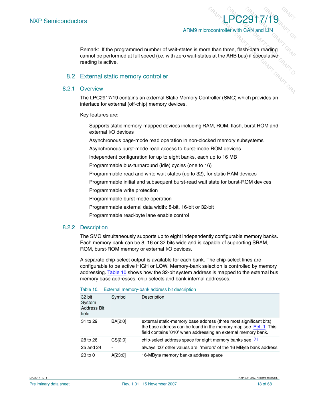
External static memory controller
External memory-bank address bit description
External static-memory controller pin description
External memory timing diagrams
External memory controller pins
External static-memory controller clock description
Reading from external memory
Writing to external memory
Reading/writing external memory
General subsystem clock description
Chip and feature identification
General subsystem
System Control Unit SCU
Peripheral subsystem clock description
Symbol Direction Bit position Description Default Polarity
Peripheral subsystem
Event-router pin connections
Timer
Watchdog timer clock description
Pin description
3.2 Description
3.3 Pin description
Uart pins
Timer clock description
Timer pins
UARTs
Serial peripheral interface
Uart clock description
Functional description
SPI pin description
SPI pins
Modes of operation
SPI clock description
6.1 Overview
Gpio pins
General-purpose I/O
Gpio pin description
LIN
Can pins
Can gateway
Global acceptance filter
LIN pin description
LIN controller pins
Modulation and sampling control subsystem
LIN0/1 Txdl
Synchronization and trigger features of the Mscss
Modulation and sampling control subsystem block diagram
Start ADC conditions is valid
Mscss pin description
Mscss clock description
Draft
Analog-to-digital converter
ADC block diagram
Analog to digital converter pins
ADC pin description
6 PWM
ADC clock description
PWM block diagram
Synchronizing the PWM counters
PWM pins
Timers in the Mscss
Master and slave mode
PWM pin description
Mscss timer 1 pin
Power, clock and reset control subsystem
Mscss timer-clock description
Pause pin for Mscss timer
Pcrss block diagram
PCR subsystem clock description
Clock Generation Unit CGU
CGU base clocks
Number Name Frequency Description MHz
Block diagram of the CGU
Structure of the clock generation scheme
PLL functional description
PLL block diagram
CGU pins
CGU pin description
Reset Generation Unit RGU
Reset output configuration
Power Management Unit PMU
RGU pins
RGU pin description
DRA
Vectored interrupt controller
PMU pin description
Limiting values
VIC pin description
VIC clock description
Thermal characteristics
Symbol Parameter Conditions Min Typ Max
Static characteristics
Static characteristics
Input pins and I/O pins configured as input
INL
Analog-to-digital converter supply
VDDA5V FSR
LSB
Dynamic characteristics
Dynamic characteristics
Power-up reset
Symbol Parameter Conditions Min Typ Max Unit
UnitDRAFT
Jitter Specification
Can TXD pin Cycle-to-cycle jitter Peak-to-peak value
Package outline
Package outline SOT486-1 LQFP144
Through-hole mount packages
Soldering
Introduction
Surface mount packages
Wave soldering
Volume mm3 350 235 220 Lead-free process from J-STD-020C
Temperature profiles for large and small components
SnPb eutectic process from J-STD-020C Package thickness mm
CPGA, Hcpga
Package related soldering information
Mounting Package1 Soldering method Wave Reflow2 Dipping
DBS, DIP, HDIP, RDBS, SDIP, SIL
Mounting
Abbreviations
Abbreviations list
Abbreviation Description
References
Document ID Release date Data sheet status
Revision history
Revision history
Legal information
Contact information
Contents
Contact information Contents
Soldering
Package outline