GM47/GM48
Publication number LZT 123 7263 R1C
All rights reserved
Contents
14.1 Digital to Analogue Converter DAC 14.2
Where to Install the Module
Digital Ground Dgnd
VIO 2.75V Supply
Conventions AT Command Syntax AT Response Syntax
Ericsson Master Reset 109
Command Line Editing Character Backspace 104
Blind Dial Delay Control 104
Connection Completion Timeout 105
Select Service for MO SMS Messages 170
Select Bearer Service Type 153
Quality of Service Profile Minimum Acceptable 164
Quality of Service Profile Requested 166
Restore SMS Settings 202 12.11
Command Echo 198 12.7
Reset to Default Configuration 200 12.9
Switch to 07.10 Multiplex Protocol 200 12.10
Send Command 262 15.10
Ericsson Settings Number 242 14.11
Select Service for MO SMS Messages 251 15.3
Service Centre Address 253 15.5
Supplementary Service Notification 328 18.17
Advice of Charge 309 18.5
M2M Supplementary Service Dispatch 313 18.10
M2M Supplementary Service Indications 314 18.11
Part 1 Overview
Page
Manual Structure
Introduction
Target Users
Prerequisites
Part 4 Using AT Commands
About the GM47/GM48 Family
GM47/GM48 Modules
GM47 in a Communication System
Interface between the Module and the Application
Gmsk
Features
Short Message Service
Average Power Consumption
Service and Support
Precautions
Abbreviation
Abbreviations
THD
Part 2 Developer’s Kit
Page
Overview
Contents of the Kit
Module connections to the developer’s board
General Functioning of the Kit
Power supply connection and the on-board voltages
Audio signals, connection and routing
Front view
Using the Developer’s Kit
Start up Check List
Developer’s board overlay
Developer’s Board Overlay
SW4 Service
Jumpers, Switches and Connectors
Dcio
ON/OFF
EAR
Micn Bearn Bearp Micp PCM
Pcmuld Pcmdld Pcmclk Pcmsync Dgnd Pcmin Pcmout System
Simvcc Simrst Simclk Simdat Simpresence Simgnd
Test
System connector pin assignments
System Connector Pin Assignments
Part 3 Integrating the Module
Page
Interface Description
Mechanical Description
Dimensions of the GM47
Physical Dimensions
GM47, viewed from underneath
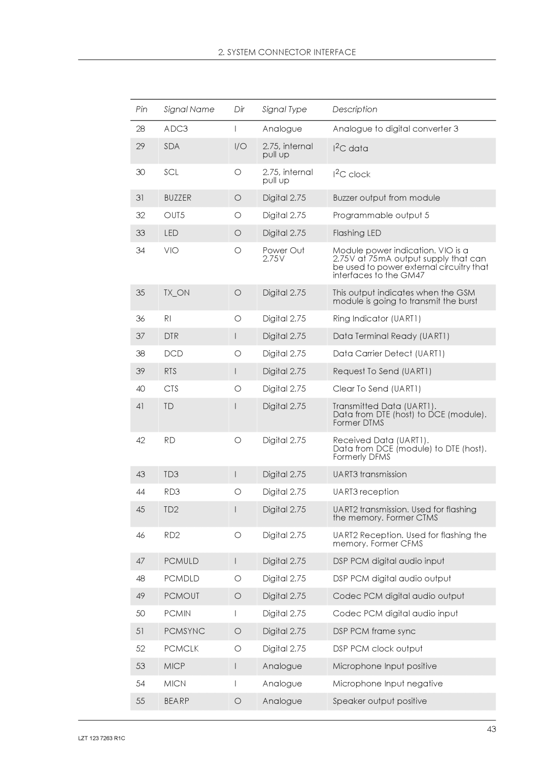
System Connector Interface
VCC
Buzzer
ADC3
SDA
SCL
Agnd
General Electrical and Logical Characteristics
Afms
Atms
Grounds
VCC Regulated Power Supply Input
Parameter Mode
ON/OFF and External Power Signal
Times are defined as follows
ON/OFF timing and VIO performance
Analogue Audio
Rxpga
Output at Afms for 3dBm0 at Pcmin
Output at BEARN/BEARP for 3dBm0 at Pcmin
AUX AMP
Microphone connections to the module
Table below shows the audio signal levels for Afms
Speaker Signals
PCM Digital Audio
Electrical characteristics
Pcmdld to Pcmin Pcmuld to Pcmout
16-bit data word format
16-bit word within 24-bit frame
Pcmclk Pcmsyn Pcmout
Serial Data Interfaces
OFF
RD, TD RTS, CTS, DTR, DCD, RI
Table below shows the switching times
UART2 TD2, RD2
Simdata
SIM Card Related Signals
RD is used to send data to your application via UART3
Simvcc
SIM Detection Simpresence
LED states shown below, are hard coded
Service/Programming
Buzzer
12 LED
Following circuit should be used to connect an LED
General Purpose Digital I/O Ports
ADC2
General Purpose Analogue I/O Ports
DAC
ADC1
DAC loads
Txon Burst Transmission
External I 2C Serial Control Bus
Vrtc
Real Time Clock
10 RTC connections
Antenna Connector
Hints for Integrating the Module
Safety Advice and Precautions
Installation of the Module
How to Install the Module
Antenna
Antenna Type
Possible Communication Disturbances
Mechanical Specifications
Technical Data
Environmental specifications
Declaration of Conformity
FCC Certificate
Part 4 Using AT Commands
Page
Syntax Description
Introduction to AT Commands
Example! ATL=0CR sets the volume of the speaker
Crokcr final result code
Example! AT+CFUN=0CR powers down the module
Example! AT+CSCS?CR show current character set
CROKCRfinal result code response
Remote station busy
Command executed, no errors
Invalid command or command line too long
No dialling possible, wrong mode
Error Codes
2 +CMS Error Message Service Failure Result Code
SMS Text Mode
Examples on How to Use the AT Commands
+CMTI SM,2
Reading messages is performed as in PDU mode
AT+CMGL=ALL
Gprs Communication
GM47/GM48 INTEGRATOR’S Manual
See 3.26, AT+CPIN PIN Control
Call Control
PIN Control
Answer Incoming Call
No Dial Tone
ATD Dial
Busy
Dialstring Description
ATD07747008670 AT+VTS=4
Included for compatibity. No functionality
Signals the MS to terminate an active call
ATH Hang up
ATL Monitor Speaker Loudness
ATP Select Pulse Dialling
ATO Return to Online Data Mode
ATT Select Tone Dialling
10 AT+CHUP Hang up Call
ATX Call Progress Monitoring Control
During a call set-up
AT+CMOD?
11 AT+CMOD Call Mode
AT+CMOD=?
13 AT+VTS Dtmf and Tone Generation
12 AT+CVHU Voice Hang-Up
Ascii
Dtmf
100
ATQ Result Code Suppression
Control and Status
ATS0 Automatic Answer Control
ATS3?
ATS3 Command Line Termination Character
ATS2 Escape Sequence Character
ATS2?
ATS4?
ATS4 Response Formatting Character
Included for compatibility. No functionality
ATS5 Command Line Editing Character Backspace
ATS6 Blind Dial Delay Control
Immediately preceding character
Connection is aborted
ATS7 Connection Completion Timeout
ATS8 Comma Dial Modifier Delay Control
Connection being established. If this time is exceeded then
AT*ECAM=?
10 ATS10 Automatic Disconnect Delay Control
11 AT*ECAM Ericsson Call Monitoring
AT*ECAM?
Control and Status
AT*EDST?
This command sets the daylight saving time hours
12 AT*EDST Ericsson Daylight Saving Time
Ecam
AT*EMAR=?
13 AT*EMAR Ericsson Master Reset
AT+CLCK
14 AT*EPEE
15 AT*ESMM Ericsson Settings Minute Minder
Inserted and accepted
AT+CALA?
16 AT+CALA Set Alarm
AT+CALA=?
AT+CALD=?
17 AT+CALD Alarm Delete
This command removes an active alarm
Unsolicited result codes +CALV n
AT+CCLK=?
18 AT+CCLK Set Clock and Date
+CCLK 00/01/01,225448+00 AT+CCLK=19/11/02,093000+00
AT+CCLK?
20 AT+CFUN Set Phone Functionality
19 AT+CEER Extended Error Report
Information given by the GSM network in text format
AT+CIND?
21 AT+CIND Indicator Control
AT+CIND=?
23 AT+CMEE Mobile Equipment Error
22 AT+CLAC List all available AT Commands
AT+CMER?
24 AT+CMER Mobile Equipment Event Reporting
AT+CMER=?
Unsolicited Result Codes +CKEV key,press +CIEV ind,value
25 AT+CPAS Phone Activity Status
AT+CPAS=?
+CPAS 0,3,4,129,130,131
26 AT+CPIN PIN Control
SIM PUK2
AT+CPIN=0000
PH-SIM PIN
SIM PIN2
AT+CPWD=?
27 AT+CPWD Change Password
AT+CPWD=SC,0000,0001
Intermediate Result Codes +CR serv
28 AT+CR Service Reporting Control
During the handshake phase
29 AT+CRC Cellular Result Code
Unsolicited Result Codes +CRING type
30 AT+CSAS Save Settings
AT+CSAS=?
AT+CSQ=?
31 AT+CSQ Signal Strength
AT+CSQ +CSQ 13,99
AT+CSQ
AT+CTZU=?
32 AT+CTZU Automatic Time Zone Update
Setting fails in an ME error, +CME Error err is returned
AT+CTZU?
128
AT*E2EAMS=?
Audio
AT*E2EAMS Ericsson M2M Audio Profile Modification
AT*E2EAMS?
Audio diagram of the Codec
Configure current profile pr1 to pr21
Mute
Volume Description MaxVolume
AT*E2EAMS?
AT*E2EAMS=? *E2EAMS=0-21,255 Current default profile is
AT*E2APR=?
AT*E2APR= Error
AT*E2APR M2M Audio Profile Manipulation
AT*E2APR?
AT*E2APR? *E2APR
E2APR= 0-4,0-2,0-2 Current default profile is profile
AT*EALR=?
Ericsson Audio Line Request
ATMS,AFMS
AT*EALR? Ealr
AT*EAMS?
Ericsson Audio Mode Selection
AT*EAMS=?
AT*EARS?
Ericsson Audio Ring Signal
AT*EARS=?
Ericsson Local Audio Mode
AT*E2PHFB Portable Handsfree Button Sense Enable
Ericsson Music Mute Indication Request
Ericsson Microphone Mode
Eprr
10 AT*EPRR Ericsson Personal Ring Type Read
AT*EPRR=?
Reserved. Not supported
11 AT*EPRW Ericsson Personal Ringtype Write
Beep. Not supported
AT*ERIL? Eril
12 AT*ERIL Ericsson Ring Level Set
AT*ERIL=?
AT*ERIN=?
13 AT*ERIN Ericsson Ring Set
AT*ERIN=
AT*ERIN?
AT*ERIP=?
14 AT*ERIP Ericsson Ring Signal Playback Command
Refer to the AT*ERIN command for the sound type parameter
AT*ERIP =
15 AT*ESMA Ericsson Set Message Alert Sound
16 AT*ESOM Ericsson Settings Own Melody
Melody 1 4. Default setting
AT*EXVC?
17 AT*EXVC
AT*EXVC=?
ATM=?
18 ATM Monitor Speaker Control
Modem and is only included for compatibility
ATM?
152
AT+CBST=?
Select Bearer Service Type
Data CSD/HSCSD
AT+CBST?
Name Description
AT+CRLP=?
Radio Link Protocol
AT+CRLP?
+CRLP
AT+CRLP? +CRLP 61,61,48,6,0 +CRLP 120,120,48,6,2,3
+CGACT=?
Data Gprs
AT+CGACT PDP Context Activate or Deactivate
+CGACT?
+CGATT?
AT+CGATT Gprs Attach or Detach
+CGATT=?
+CGDATA=?
AT+CGDATA Enter Data State
+CGDCONT=?
AT+CGDCONT Define PDP Context
+CGDCONT?
CRLF+CGDCONT
APN
+CGEREP?
AT+CGEREP Gprs Event Reporting
+CGEREP=?
+CGPADDR=?
AT+CGPADDR Show PDP Address
+CGPADDR
CRLF+CGPAD
+CGQMIN?
AT+CGQMIN Quality of Service Profile Minimum Acceptable
+CGQMIN=?
165
+CGQREQ?
AT+CGQREQ Quality of Service Profile Requested
+CGQREQ=?
167
GM47/GM48 INTEGRATOR’S Manual
AT+CGREG?
AT+CGREG Gprs Network Registration Status
AT+CGREG=?
+CGSMS?
10 AT+CGSMS Select Service for MO SMS Messages
+CGSMS=?
AT+CHSC=?
Data Hscsd
Hscsd Current Call Parameters
AT+CHSC
AT+CHSD
Hscsd Device Parameters
AT+CHSD=?
AT+CHSN?
Hscsd Non Transparent Call Configuration
AT+CHSN=?
AT+CHSR?
Hscsd Parameters Report
AT+CHSR=?
AT+CHSU=?
Hscsd Automatic User Initiated Upgrading
Itermediate Result Codes +CHSR rx,tx,aiur,coding
AT+CHSU?
176
AT*EENMEA?
AT*EENMEA Nmea GPS Mode on UART2
GPS Interoperability
Uart
AT*E2NMPR=?
AT*E2NMPR Ericsson M2M Set Nmea GPS Port Rate
AT*E2NMPR=? *E2NMPR=0-10 Port rate currently set
AT*E2NMPR?
Set GPS/NMEA port rate to 4800 baud
180
AT*E2FAX?
Fax
AT*E2FAX Ericsson M2M Fax Comm. Baud Rate Modification
E2FAX=
E2FAX Current default setting is 19200 baud
Low Level Fax Commands
Sets default RS232 setting to 9600 baud
10.1 AT
10.2 AT&F Set to Factory Defined Configuration
Supports AT commands, it returns an OK final result code
Identification
10.6 AT+CGMM Read MS Model Identification
10.4 AT List all Supported AT Commands
Lists all the commands supported by the MS
10.5 AT+CGMI Read MS Manufacturer Identification
AT+CGMR
10.7 AT+CGMR Read MS Revision Identification
BVGM47
About the software version
10.9 AT+GMI
10.8 AT+CGSN Read MS Product Serial Number Identification
10.11 AT+GMR Read Revision Identification
10.10 AT+GMM Read Model Identification
R2A009prgCXC1122112
+CGACT 1,0
Configuration Settings on Channel 0 &C
10.12 ATI Identification Information
CXC1122112
189
190
11.1 AT*E2IO Ericsson M2M Input/Output Read/Write
Input/Output
AT*E2IO=?
192
Read
False
Unsolicited Result Codes *E2IO source, io, val
Reading an I/O
Writing in an Output
Checking an I/O status
Configuring an I/O
Checking an Input Trigger
Triggering an Input
Determines the behaviour of the carrier detect
Interface
12.3 AT&D Circuit 108 DTR Response
12.4 AT&S Circuit 107 DSR Response
Phone
12.5 AT+WS46 Mode Selection
12.6 ATE Command Echo
Determines the behaviour of the data set ready signal
List of result codes
12.7 ATV DCE Response Format
12.9 AT+CMUX Switch to 07.10 Multiplex Protocol
12.8 ATZ Reset to Default Configuration
201
Result code, if this is not automatically determined Not
12.10 AT+CRES Restore SMS Settings
Parameters, cannot be restored
12.11 AT+ICF Cable Interface Character Format
AT+IFC=?
12.12 AT+IFC DTE-DCE Local Flow Control
+ICF 3,3
AT+IFC?
Transmitted
12.14 AT+IPR Cable Interface Port Command
12.13 AT+ILRR Cable Interface Local Rate Reporting
Specifies whether or not the extended-format +ILRRrate
AT*E2SPI=?
12.15 AT*E2SPI Serial Peripheral Interface
E2SPI
AT*E2SPI?
AT*E2SPI=0
AT*E2ESC?
12.16 AT*E2ESC M2M Escape Sequence Guard Time
AT*E2ESC=?
208
AT*E2CD=?
Network
13.1 AT*E2CD Ericsson M2M Cell Description
AT*E2CD?
According to GSM 04.18 V8.6.0, the coding of the timing
13.2 AT*E2EMM Ericsson M2M Engineering Monitoring Mode
AT*E2EMM=1
AT*E2EMM=7
Responses. Default value is
215
216
13.4 AT*EALS Ericsson Request ALS Status
13.3 AT*E2SPN M2M Service Provider Indication
SIM
SIM
13.5 AT*ECSP Ericsson Customer Service Profile
AT*ECSP=?
AT*EPNR=?
13.6 AT*EPNR Ericsson Read SIM Preferred Network
Epnr 10,27801
13.7 AT*EPNW Ericsson Write SIM Preferred Network
AT*EPNW=?
SSN
13.8 AT*E2SSN Ericsson M2M SIM Serial Number
AT*E2SSN?
AT*E2SSN=?
AT*ESLN=?
13.9 AT*ESLN Ericsson Set Line Name
Sets the name tag for a selected line
AT*ESLN? Esln
234157411545420
13.10 AT+CIMI Subscriber Identification
13.11 AT+CLCK
Attached to the ME
Baoc bar all outgoing calls
LF+CNUM
13.12 AT+CNUM Subscriber Number
+CPWD
AT+CNUM
AT+COLP=?
13.13 AT+COLP Connected Line Identification Presentation
UDI
AT+COLP?
Disable
AT+COPS?
13.14 AT+COPS Operator Selection
AT+COPS=?
AT+CREG?
13.15 AT+CREG Network Registration
AT+CREG=?
AT*ECPI=?
13.16 AT*ECPI Ciphering Indicator
+CREG 0,1
AT*ECPI?
231
AT*E2NBTS?
13.17 AT*E2NBTS Ericsson M2M Neighbour BTS
AT*E2NBTS=?
233
234
14.1 AT*E2PBCS Ericsson M2M Phonebook Check Sum
Phonebook
14.2 AT*ESAG Ericsson Add to Group
AT*ESCG=?
14.3 AT*ESCG Ericsson Create Group
AT*ESCN=?
14.4 AT*ESCN
238
14.6 AT*ESDI Ericsson Delete Group Item
14.5 AT*ESDG Ericsson Delete Group
AT*ESGR=?
14.7 AT*ESGR Ericsson Group Read
14.8 AT*EGIR Ericsson Group Item Read
AT*ESGR
AT*ESIL=?
14.9 AT*ESIL Ericsson Silence Command
Is in silent mode, all sounds from the MS are prevented
AT*ESIL?
AT*ESNU?
14.10 AT*ESNU Ericsson Settings Number
AT*ESNU=?
+CPBF=?
14.11 AT+CPBF Phonebook Find
14.12 AT+CPBR Phonebook Read
+CPBF
244
AT+CPBS?
14.13 AT+CPBS Phone Storage
AT+CPBS=?
AT+CPBW=?
14.14 AT+CPBW Phonebook Write
AT*ECAW=?
14.15 AT*ECAW Ericsson Callers Allowed Write
AT*ECAR=?
14.16 AT*ECAR Ericsson Callers Allowed Read
Cluid
AT*ECAR=
If listing fails in a ME +CME Error err is returned
250
15.3 AT+CPMS Preferred Message Storage
Short Message Services Point to Point
15.2 AT+CGSMS Select Service for MO SMS Messages
15.1 AT+CPIN PIN Control
+CPMS ME,0,40,SM,1,15,ME,0,40
+CPMS ME,SM,ME,SM,ME,SM
AT+CSCA=?
15.4 AT+CSCA Service Centre Address
AT+CPMS=sm,sm,sm +CPMS 1,15,1,15,1,15
AT+CSCA?
AT+CMGF=?
15.5 AT+CMGF Message Format
+CSCA 44385016005,145
AT+CMGF?
AT+CMGW=?
15.6 AT+CMGW Write Message to Memory
ESC
Text Mode
15.7 AT+CMGS Send Message
ESC Error
AT+CMGS=?
258
259
AT+CSMP=17,167,0,0 AT+CMGS=+447747008670 Test SMS� +CMGS
15.8 AT+CMSS Send From Storage
AT+CMSS=?
Command is
+CMGC
15.9 AT+CMGC Send Command
AT+CMGC=?
Text is entered ctrl-Z/ESC
AT+CNMI?
15.10 AT+CNMI New Message Indications to TE
AT+CNMI=?
Unsolicited Result codes
266
+CBM
AT+CMGR=?
15.11 AT+CMGR Read Message
Display cell broadcast messages AT+CNMI=3,0,2,0,0
AT+CMGR=
269
Successful and CBM storage
+CMGR
271
272
Compressed text not supported
AT+CMGL=?
15.12 AT+CMGL List Message
R1A100 CXC1122112
+CMGL
275
AT+CMGL?
AT+CMGL
277
278
279
AT+CSDH?
15.14 AT+CSDH Show Text Mode Parameters
15.13 AT+CMGD Delete Message
AT+CMGD=?
AT+CSMP?
15.15 AT+CSMP Set Text Mode Parameters
AT+CSMP=?
15.16 AT+CSCS Select Character Set
AT+CSMS=?
15.17 AT+CSMS Select Message Service
+CSMS
AT+CSMS?
SMS Error
15.18 AT*E2SMSRIRing indicator for SMS
AT*E2SMSRI=?
RI is disabled for incoming SMS messages. Default value
286
See 15.10, AT+CNMI New Message Indications to TE
Short Message Services Cell Broadcast
16.1 AT+CNMI New Message Indications to TE
16.2 AT+CSCB Select Cell Broadcast Message Type
288
AT*E2STKS=?
SIM Application Toolkit
STK
AT*E2STKS?
17.3 AT*E2STKD M2M STK Display Text
Display Text Error
AT*E2STKD=?
AT*E2STKG=?
17.4 AT*E2STKG M2M STK Get Inkey
Values follow GSM 11.14 standard
GET Inkey
292
Input
17.5 AT*E2STKI M2M STK Get Input
AT*E2STKI=?
Answer Description
295
17.6 AT*E2STKL M2M STK Select Item
Select Item Error
AT*E2STKL=?
Maximum length is fixed
Maximum length is fixed
UP Menu Error
17.7 AT*E2STKM M2M STK Set Up Menu
AT*E2STKM=?
GSM default alphabet
Command
17.9 AT*E2STKC M2M STK Set Up Call
Parameters have no default values
AT*E2SKTN command. The ME answers with OK, or Error
No response from user. It corresponds to ‘12’ no response
ME passes the alphaid within Send Short Message
17.10 *E2STKE STK Send Short Message
Unsolicited Result Code
E2STKE coding, textlength , alphaid
17.11 *E2STKP STK Send SS
17.12 *E2STKU STK Send Ussd
Unsolicited Result Code
17.14 AT*E2STKTO SIM Application Toolkit Settings
E2STKR indicator
17.13 *E2STKR STK Refresh
Unsolicited result code *E2STKTO command
18.1 AT+CPIN PIN Control
Supplementary Services
18.2 AT+CACM Accumulated Call Meter
AT+CAMM?
18.3 AT+CAMM Accumulated Call Meter Maximum
AT+CAMM=?
AT+CAOC?
18.4 AT+CAOC Advice of Charge
AT+CAOC=?
SEK
18.5 AT+CPUC Price Per Unit and Currency Table
AT+CPUC?
AT+CPUC=?
AT*EDIF?
18.6 AT*EDIF Ericsson Divert Function
With the unsolicited result code *EDIF
Edif
AT*EIPS?
18.7 AT*EIPS Identity Presentation Set
Unsolicited Result Codes *ELIPalpha tag *EOLPalpha tag
AT*EIPS=ID
AT*ELIN=?
18.9 AT*E2SSD M2M Supplementary Service Dispatch
18.8 AT*ELIN Ericsson Line Set
AT*ELIN?
Refer to GSM 02.30 for Public MMI services and codes
18.10 AT*E2SSI M2M Supplementary Service Indications
Ssicallbarred
Ssisimerror
Ssinetworkproblem
Ssinumbererr
Multiparty
Bearerservice
Teleservice
Bsallpadaccesscaservices
BS12KBITUNRESTRICTEDDIGITAL
Bsallsynchronousservices
Tsalldataservices
Tsallteleservicesexceptsms
Ssstatuspra
Temporarydefaultrestricted
Temporarydefaultallowed
Ssstatusprovisioned
+CCFC
18.11 AT+CCFC Call Forwarding number and Conditions
AT+CCFC=?
Default value if ‘+’ is in sca
AT+CCWA?
18.12 AT+CCWA Call Waiting
AT+CCWA=?
Unsolicited Result Codes +CCWA number, type, class
Default value is
AT+CCWA=? +CCWA
18.13 AT+CHLD Call Hold and Multiparty
AT+CHLD=?
Integer type equals to numbers entered before Send
AT+CLIP?
18.14 AT+CLIP Calling Line Identification
AT+CLIP=?
AT+CLIR?
18.15 AT+CLIR Calling Line Identification Restriction
+CLIP number,type
+CLIP 07747008670,129,,,Matt L,0
Presentation indicator is used according to
AT+CSSN?
18.16 AT+CSSN Supplementary Service Notification
AT+CSSN=?
Enable the +CSSU result code presentation status in the TA
AT+CUSD?
18.17 AT+CUSD Unstructured Supplementary Service Data
AT+CUSD=?
+CUSD0 OK
Different alternatives are shown below
AT+CUSD=1,*#100# +CUSD 0,07787154042
+CUSD0,ALARM
Alphabetical Listing of AT Commands
AT*E2STKS
AT*E2STKL
AT*E2STKM
AT*E2STKN
AT*ESDI
AT*ESCG
AT*ESCN
AT*ESDG
AT+CHLD
AT+CGQREQ
AT+CGREG
AT+CGSMS
AT+CPBS
AT+CPAS
AT+CPBF
AT+CPBR
ATA
AT+IPR
AT+VTS
AT+WS46