1. INTRODUCTION
12v
DC Power Socket,
Input 10..15V
5V to development
board circuits
5V | 2V7 |
reg. | reg. |
3V8
reg.
Vcc
Switched |
| VIO present |
when VIO |
| LED |
present |
|
|
2V7 To development ![]() board & interface circuits
board & interface circuits
VIO
GM47
3V8 VCC
+ -
TP4 TP5
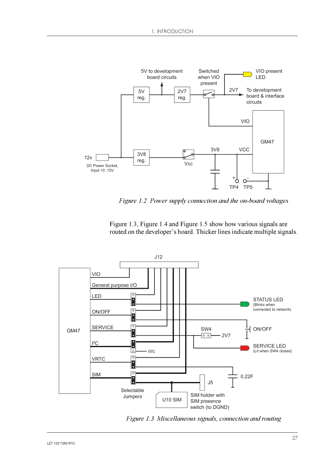
Figure 1.2 Power supply connection and the on-board voltages
Figure 1.3, Figure 1.4 and Figure 1.5 show how various signals are routed on the developer’s board. Thicker lines indicate multiple signals.
GM47
J12
VIO
General purpose I/O
LED |
|
|
| STATUS LED |
|
|
|
| |
|
|
|
| (Blinks when |
ON/OFF |
|
|
| connected to network) |
|
|
|
| |
SERVICE |
|
| SW4 | ON/OFF |
|
|
| ||
|
|
| 2V7 |
|
I²C |
|
|
| SERVICE LED |
|
|
|
| |
|
| n/c |
| (Lit when SW4 closed) |
VRTC |
|
|
|
|
SIM |
|
|
| 0.22F |
|
|
|
| |
|
|
| J5 |
|
| Selectable |
|
|
|
| Jumpers |
| SIM holder with |
|
| U10 SIM |
|
| |
|
| SIM presence |
| |
|
|
|
| |
|
|
| switch (to DGND) |
|
Figure 1.3 Miscellaneous signals, connection and routing
27
LZT 123 7263 R1C
