Series
Warranty
Page
Page
Table Of Contents
Table of Contents
682XXB/683XXB MM Iii
Power Level Accuracy and Flatness Tests
Calibration
Troubleshooting
Appendix a Test Records
Chapter General Information Table of Contents
Page
Scope of Manual
Introduction
3DESCRIPTION
Frequency Output Power Model GHz Step Attenuator
General
Information Models
General Identification Information Number
With Option 15B High Power Installed
4IDENTIFICATION
Number
Information Manual
Electronic Manual
Related Manuals
General Options Information
7OPTIONS
Option 16, High-Stability Time Base. Adds an ovenized
General Level Information Maintenance
Maintenance
8LEVEL
General Preventive Information Maintenance
Static-Sensitive Component Handling Precautions
General Start UP Information Configuration
Configurations
11STARTUP
General Recommended Information
12RECOMMENDED Test
Equipment
Usage
Specification MANUFACTURER/MODEL
General Exchange Information
Printed Circuit Board Assemblies
General Information
RF Components
682XXB/683XXB with Front Handles Installed
682XXB/683XXB without Front Handles Installed
General Anritsu Information
Chapter Functional Description Table of Contents
Table of Contents
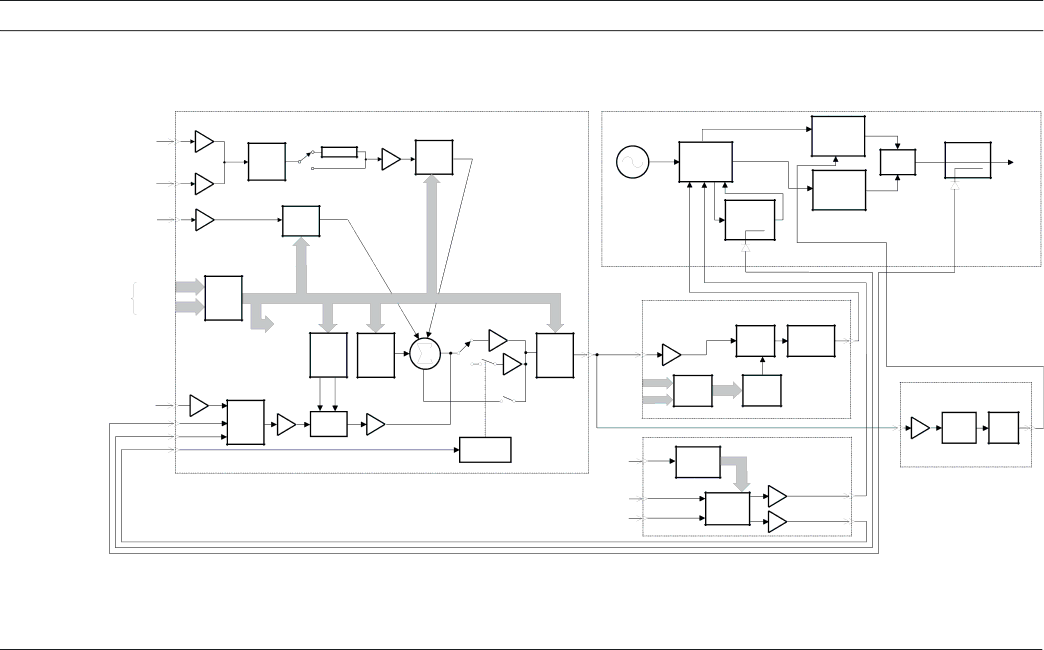
Subsystems
682XXB/683XXB Major
Description
Functional
Analog
Front Panel Rear Panel
Power Supply
Front Panel
Front Panel Control
Instruction
Analog
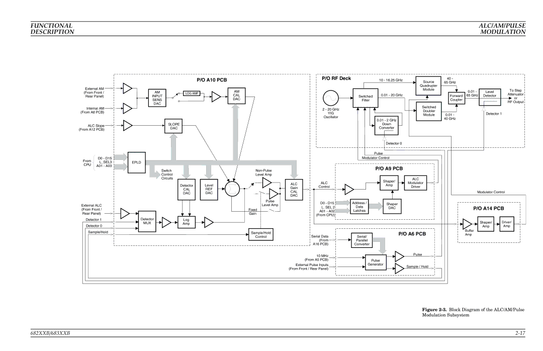
ALC/AM/Pulse
Description Synthesis
Overall
A4 Coarse Loop
Switched Filter
A5 Fine Loop
A11 FM A7 YIG Loop
RF OUT Coarse Loop Fine Loop
MHz
20 to 40 GHz
01 to 2 GHz
40 to 65 GHz
To 2.2 GHz
Frequency
Functional ALC/AM/PULSE Description Modulation
4ALC/AM/PULSE
Modulation
ALC Slope
External Leveling
RF Deck
682XXB/683XXB
Power Sweep
Amplitude Modulation
Pulse Modulation Operation
5RF Deck Assemblies
Functional RF Deck Description
RF Deck Con- All 682XXB/683XXB RF deck assemblies contain a
RF Path for 20 GHz Models
U r c e Q u a d r u p le r M o d u le
Functional RF Deck Description Assemblies
Functional RF Deck Description
Down
ALC PCB
GHz Models
Module
Switched Doubler Module ND40843
RF Deck
GHz Models SQM P/N
GHz Models SQM P/N D28185
Functional RF Deck Description
Attenuator
682XXB/683XXB MM 31/2-32
Page
Chapter Performance Verification Table of Contents
Frequency Modulation Tests
1INTRODUCTION
4CONNECTOR and KEY
Recommended Test
Test Records
Performance Recommended Verification
Any common source All tests
Levels
Performance
Not Available 40.0 50.0 GHz DBm
Performance
Test
Performance
Performance Frequency Verification
7FREQUENCY
Synthesis Tests
Performance Frequency Verification
Performance Frequency Verification
Models
GHz 2.2 GHz for 68XX5B Models
MHz to £50 MHz
Harmonic and Harmonic Related MHz to 2.2 GHz 68XX5B
MHz to £2 GHz
GHz 2.2 GHz for 68XX5B To £20 GHz
Performance
System
Signals from 2 to 20 GHz
Test Procedure 2 to 10 GHz
Following procedure lets you measure the 11 to
Performance
Performance Single Sideband Verification Phase Noise Test
Phase Noise Test
10SINGLE Sideband
Performance Single Sideband Verification
Phase Noise Test
CW Carrier Offset From
Frequency Carrier Specification
Performance Single Sideband Verification
Verification Flatness Tests
Power Level
Accuracy
Flatness Tests
Performance
Frequency Control
Performance
Performance Amplitude Verification Modulation Test
Amplitude
Modulation Test
Performance Amplitude Verification Modulation Test
Performance Amplitude Verification Modulation Test
Performance Frequency Verification Modulation Tests
13FREQUENCY
Modulation Tests
Unlocked Wide FM Mode
Unlocked Narrow FM Mode
240
Locked FM Mode
Locked Low-Noise FM Mode
Performance Frequency Verification Modulation Tests
Rise TIME, Fall TIME, OVERSHOOT, and Level
Performance Pulse Modulation Tests Verification
Modulation
Pulse Leveling Accuracy
Performance Pulse Modulation Tests Verification
Pulse Modulation
Verification Video Feedthrough
Test Video
Feedthrough
Following procedure lets you measure the video
16PULSE Modulation
Test RF ON/OFF
Ratio
Verification RF ON/OFF Ratio
Performance
Performance Phase Verification Modulation Tests
17PHASE Modulation
Tests
Deviation in rad
Wide M Mode
Narrow M Mode
Chapter Calibration Table of Contents
FM Calibration Firmware Version
During performance verification testing see or as a result
Calibration
Calibration Following
Any common source All procedures
ALC PCB
6INITIAL Setup
Calibration Initial Setup
T1678 Serial Interface
682XXB / 683XXB IBM-Compatible PC
Calibration Initial Setup
Calibration Initial Setup
Calibration Initial Setup
Calibration Initial Setup
Calibration Initial Setup
Preliminary
Preliminary
Preliminary
Preliminary
Preliminary
Switched Filter
Switched Filter
Calibration Shaper Calibration
Shaper Calibration
Limiter DAC
Shaper DAC Adjustment
DAC
Switched Filter
RF Level
ALC Slope
10ALC Slope
Models 683XXB with Firmware Version 1.01 to
GHz
ALC Slope
ALC Slope
IBM-Compatible PC
Transmission and Select Input NON-RATIO a
ALC Slope Adjustment Waveform Display
ALC Slope
ALC Bandwidth
ALC Bandwidth
ALC Bandwidth
12AM Calibration
DMM
Calibration DAC to provide the correct amount
Calibration
Calibration
13FM Calibration
Models 682XXB/683XXB with Firmware Versions 1.01 to
Models 682X5B/683X5B with Firmwave Version
Calibrate the FM Meter circuit, 2 calibrate the FM
Calibration
Bessel
Calibration
Calibration
Calibration
BNC
CPU PCB
Calibration
Calibration
Bessel
Calibration
Calibration
14PHASE Modulation
Phase Modulation
Calibration Procedure
Phase Modulation
Phase Modulation
Phase Modulation
Phase Modulation
Chapter Troubleshooting Table of Contents
Page
Messages
Error
Troubleshooting
Error Message Troubleshooting Number
SELF-TEST
Self-Test Error Messages 2
682XXB/683XXB Models with SDM
Error and Warning
Troubleshooting Status Messages
Error Message Description
ERR
Message
OVN Cold
Malfunctions not Displaying
Troubleshooting AN Error Message
Troubleshooting Test Point Locations
Connector
Signal Generator Will Not Turn On Operate light is OFF
Troubleshooting Tables
Signal Generator Will Not Turn On Operate light is on
No Pulse Modulation of the RF Output
Malfunctions Not Displaying an Error Message 4
683XXB Setup
682XXB Setup CW/SWEEP Select Step F1 40.0 GHz
Malfunctions Not Displaying an Error Message 6
Internal DVM Tests
Regulated
Error 105 Power Supply Voltages out of Regulation
Value
Point To Step
Error Messages 105 and 106 2
15VG Supply Problems
15VA Supply Problems
15VLP Supply Problems
15VFM Supply Problems
18VT Supply Problems
43VT Supply Problems
+24VH Supply Problems
Error 106 Power Supply not Locked
Power Supply not Locked and Error 148 is not Displayed
Power Supply not Locked and Error 148 is Displayed
A3 Reference Loop
Error 108 Crystal Oven Cold
A5 Fine Loop
Error 111 Fine Loop Osc Failed
682XXB/683XXB Measured Frequency CW Frequency At A5J1
Step
Error 112 Coarse Loop Osc Failed
682XXB/683XXB Measured
CW Frequency Frequency at A4J3
A7 YIG Loop
Down Converter
Error 114 Down Converter LO not Locked
A11 FM PCB
Error 116 FM Loop Gain Check Failed
A12 Analog Instruction
A10 ALC
Error 142 Sample and Hold Circuit Failed
Error 143 Slope DAC Failed
YIG-tuned Oscillator
682XXB Setup CW/SWEEP Select Step F1 2.000 GHz
A13TP3 +6V A13TP5 +8V A13TP6 A13TP7
682XXB Setup CW/SWEEP Select Step F1 0.010 GHz
Error 128 .01-2 GHz Unleveled
Unleveled with no/low output power
Troubleshooting
Error 129 Switched Filter or Level Detector Failed
Unleveled with no/low output power
Troubleshooting
Voltage
Test Point Active Frequency Inactive Range
Error 135 Modulator or Driver Failed
682XXB Setup CW/SWEEP Select Step F1 20.000 GHz
Error 138 SDM Unit or Driver Failed
Test Point Active Frequency Inactive Range Voltage
Error 145 AM Meter or associated circuitry failed
Error 148 Pulse 40 MHz reference circuitry failed
Error 147 Internal FM circuitry failed
682XXB/683XXB MM 53/5-54
Page
Chapter Removal and Replacement Procedures Table of Contents
Removing and Replacing the A16 or
682XXB/683XXB assemblies, subassemblies, and components for
Removal
Replacement Procedures Covers
2REMOVING
Replacing
Chassis Covers Removal
Panel Assembly
Removal Front Panel Replacement Procedures Assembly
3REMOVING
Replacing the Front
Front Panel Assembly Removal
Replacement Procedures Removal Diagram
4REMOVING and Replacing the A3, A4, A5, or A6 PCB
Replacement Procedures Or A6 PCB
Assembly and Component Locator Diagram
Removal Replacement Procedures A7 PCB
5REMOVING
6REMOVING and Replacing the A8, A9, A10, A11, or A12 PCB
7REMOVING and Replacing the A13, A14, or A15 PCB
Replacement Procedures Or A15 PCB
8REMOVING
A17 PCB
A19 PCB
9REMOVING
Removal Rear Panel Replacement Procedures Assembly
10REMOVING
Replacing the Rear
Removal Rear Panel Replacement Procedures Assembly
Rear Panel Assembly
Removal Replacement Procedures
11REMOVING
A21 PCB
12REMOVING
A21-1 PCB
Assembly
Removal FAN Replacement Procedures
13REMOVING
Replacing the FAN
682XXB/683XXB MM A-2
Model Number
Calibration
Page
Measured Value Upper Limit
Test Procedure
Test Model Record
Frequency Synthesis Tests
Test Frequency in GHz Measured Value
Harmonic Test RF Output Signals From 2 to 20 GHz
Spurious Signals Test RF Output Signals 2 GHz
Test Procedure 11 to 20 GHz
Single Sideband Phase Noise Test
Set L1 to Max Power Min Power
Set F1 to 5.0 GHz Set L1 to Measured Power
+13.0 dBm DBm
+13 dBm DBm
+11 dBm DBm
Set L1 to Max Power Min Power Variation +11 dBm DBm
+17 dBm DBm
+15 dBm DBm
Amplitude Modulation Test
Frequency Modulation Tests
Lower Limit Measured Value Upper Limit
Lower Limit
Locked Low-Noise FM Mode
Phase Modulation Tests
Pulse Modulation Test Video Feedthrough
Pulse Modulation Test RF On/Off Ratio
Step Completion
Switched Filter Shaper Calibration
RF Level Calibration
ALC Bandwidth Calibration
AM Calibration
FM Calibration 68237B/68337B with Firmware Version 1.01 to
Wide FM Mode latness Calibration calterm
Phase Modulation M Calibration Option
Test Procedure
68245B/68345B
Spurious Signals Test RF Output Signals 2.2 GHz
Test Procedure 2.2 to 10 GHz
Harmonic Test RF Output Signals From 2.2 to 20 GHz
Test Procedure 11 to 20 GHz
DBc 84 dBc
Set F1 to 1.0 GHz Set F1 to 5.0 GHz Set L1 to Measured Power
+11 dBm DBm Maximum variation is 1.6 dB
Test Model Record
Test Model Record
Amplitude Modulation Test
Pulse Level Accuracy 1 GHz, Pulse Width = 1.0 s
Pulse Modulation Test Video Feedthrough
Test Procedure 1 GHz
Limiter DAC Adjustment Model 68245B/68345B’s with Option 15B
RF Level Calibration
FM Calibration 68245B/68345B with Firmware Version
Phase Modulation M Calibration Option
Test Procedure
68247B/68347B
Record the presence of the worst case non-harmonic
Harmonic Test RF Output Signals From 2 to 20 GHz
Test Procedure 11 to 20 GHz
DBc 82 dBc
Power Level Accuracy Test Procedure
+11 dBm DBm
Set L1 to Max Power Min Power Variation
Test Model Record
Amplitude Modulation Test
Locked Low-Noise FM Mode
Pulse Modulation Test Video Feedthrough
60 dB
Limiter DAC Adjustment Model 68247B/68347B’s with Option 15B
ALC Slope Calibration 68347B having Firmware Version 1.01 to
FM Calibration 68247B/68347B with Firmware Version 1.01 to
Phase Modulation M Calibration Option
Test Procedure
68253B/68353B
Test Frequency in GHz
Harmonic Test RF Output Signals From 2 to 20 GHz
DBc is Option 15B High Power installed
DBc 73 dBc
+ 6 dBm DBm
+ 3.5 dBm DBm
+ 10 dBm DBm
+ 7.5 dBm DBm
Amplitude Modulation Test
Locked Low-Noise FM Mode
682XXB/683XXB MM 67/A-68
Page
Limiter DAC Adjustment Model 68253B/68353B’s with Option 15B
ALC Slope Calibration 68353B having Firmware Version 1.01 to
FM Calibration 68253B/68353B with Firmware Version 1.01 to
Phase Modulation M Calibration Option
Test Procedure
68255B/68355B
Specifications for all frequencies listed above is ±100 Hz
Spurious Signals Test RF Output Signals 2.2 GHz
Measure Value
DBc 78 dBc
DBc 75 dBc
Specification is ±1.0 dB
+ 3.5 dBm DBm
Set L1 to Max Power Min Power Variation + 10 dBm DBm
+ 7.5 dBm DBm
68255B/68355B
Locked Low-Noise FM Mode
Pulse Modulation Test Video Feedthrough
682XXB/683XXB MM 87/A-88
Page
Limiter DAC Adjustment Model 68255B/68355B’s with Option 15B
ALC Bandwidth Calibration Calterm Store the Calbration Data
FM Calibration 68255B/68355B with Firmware Version
External Wide FΜ Μοδε Σενσιτιϖιτψ Χαλιβρατιον χαλτερ∝
Test Procedure
68259B/68359B
Test Frequency in GHz
Spurious Signals Test RF Output Signals 2 GHz
Harmonic Test RF Output Signals From 2 to 20 GHz
DBc 74 dBc
75 dBc
100 682XXB/683XXB MM
682XXB/683XXB MM 101
102 682XXB/683XXB MM
682XXB/683XXB MM 103
104 682XXB/683XXB MM
682XXB/683XXB MM 105
Lower Limit Measured Upper Limit Value
106 682XXB/683XXB MM
682XXB/683XXB MM 107/A-108
68259B/68359B
Page
682XXB/683XXB MM 109
ALC Slope Calibration 68359B having Firmware Version 1.01 to
110 682XXB/683XXB MM
FM Calibration 68259B/68359B with Firmware Version 1.01 to
682XXB/683XXB MM 111
112 682XXB/683XXB MM
682XXB/683XXB MM 113
114 682XXB/683XXB MM
68263B/68363B
682XXB/683XXB MM 115
116 682XXB/683XXB MM
682XXB/683XXB MM 117
118 682XXB/683XXB MM
682XXB/683XXB MM 119
+ 3 dBm DBm
120 682XXB/683XXB MM
682XXB/683XXB MM 121
122 682XXB/683XXB MM
682XXB/683XXB MM 123
124 682XXB/683XXB MM
682XXB/683XXB MM 125/A-126
Page
682XXB/683XXB MM 127
ALC Slope Calibration 68363B having Firmware Version 1.01 to
128 682XXB/683XXB MM
FM Calibration 68263B/68363B with Firmware Version 1.01 to
682XXB/683XXB MM 129
130 682XXB/683XXB MM
682XXB/683XXB MM 131
132 682XXB/683XXB MM
68265B/68365B
682XXB/683XXB MM 133
134 682XXB/683XXB MM
682XXB/683XXB MM 135
136 682XXB/683XXB MM
682XXB/683XXB MM 137
138 682XXB/683XXB MM
682XXB/683XXB MM 139
140 682XXB/683XXB MM
Set L1 to Max Power Min Power Variation + 6 dBm DBm
682XXB/683XXB MM 141
142 682XXB/683XXB MM
682XXB/683XXB MM 143
144 682XXB/683XXB MM
682XXB/683XXB MM 145/A-146
68265B/68365B
Page
682XXB/683XXB MM 147
148 682XXB/683XXB MM
FM Calibration 68265B/68365B with Firmware Version
682XXB/683XXB MM 149
150 682XXB/683XXB MM
682XXB/683XXB MM 151
152 682XXB/683XXB MM
68269B/68369B
682XXB/683XXB MM 153
154 682XXB/683XXB MM
682XXB/683XXB MM 155
156 682XXB/683XXB MM
682XXB/683XXB MM 157
158 682XXB/683XXB MM
682XXB/683XXB MM 159
160 682XXB/683XXB MM
682XXB/683XXB MM 161
162 682XXB/683XXB MM
682XXB/683XXB MM 163
164 682XXB/683XXB MM
682XXB/683XXB MM 165/A-166
68269B/68369B
Page
682XXB/683XXB MM 167
ALC Slope Calibration 68369B having Firmware Version 1.01 to
168 682XXB/683XXB MM
FM Calibration 68269B/68369B with Firmware Version 1.01 to
682XXB/683XXB MM 169
170 682XXB/683XXB MM
682XXB/683XXB MM 171
172 682XXB/683XXB MM
68275B/68375B
682XXB/683XXB MM 173
174 682XXB/683XXB MM
682XXB/683XXB MM 175
176 682XXB/683XXB MM
682XXB/683XXB MM 177
+ 2.5 dBm DBm
178 682XXB/683XXB MM
682XXB/683XXB MM 179
180 682XXB/683XXB MM
682XXB/683XXB MM 181
182 682XXB/683XXB MM
682XXB/683XXB MM 183/A-184
Page
682XXB/683XXB MM 185
186 682XXB/683XXB MM
FM Calibration 68275B/68375B with Firmware Version
682XXB/683XXB MM 187
188 682XXB/683XXB MM
682XXB/683XXB MM 189
190 682XXB/683XXB MM
68277B/68377B
682XXB/683XXB MM 191
192 682XXB/683XXB MM
682XXB/683XXB MM 193
194 682XXB/683XXB MM
682XXB/683XXB MM 195
196 682XXB/683XXB MM
682XXB/683XXB MM 197
198 682XXB/683XXB MM
682XXB/683XXB MM 199
200 682XXB/683XXB MM
682XXB/683XXB MM 201/A-202
68277B/68377B
Page
682XXB/683XXB MM 203
ALC Slope Calibration 68377B having Firmware Version 1.01 to
204 682XXB/683XXB MM
FM Calibration 68277B/68377B with Firmware Version 1.01 to
682XXB/683XXB MM 205
206 682XXB/683XXB MM
682XXB/683XXB MM 207
208 682XXB/683XXB MM
68285B/68385B
682XXB/683XXB MM 209
Fine Loop Test Procedure Standard 68X85B
210 682XXB/683XXB MM
682XXB/683XXB MM 211
212 682XXB/683XXB MM
682XXB/683XXB MM 213
+ 2 dBm DBm
214 682XXB/683XXB MM
682XXB/683XXB MM 215
216 682XXB/683XXB MM
682XXB/683XXB MM 217
218 682XXB/683XXB MM
682XXB/683XXB MM 219/A-220
68285B/68385B
Page
682XXB/683XXB MM 221
222 682XXB/683XXB MM
FM Calibration 68285B/68385B with Firmware Version
682XXB/683XXB MM 223
224 682XXB/683XXB MM
682XXB/683XXB MM 225
226 682XXB/683XXB MM
68287B/68387B
682XXB/683XXB MM 227
Fine Loop Test Procedure Standard 68X87B
228 682XXB/683XXB MM
682XXB/683XXB MM 229
230 682XXB/683XXB MM
682XXB/683XXB MM 231
232 682XXB/683XXB MM
Set L1 to Max Power Min Power Variation + 2 dBm DBm
682XXB/683XXB MM 233
234 682XXB/683XXB MM
682XXB/683XXB MM 235
236 682XXB/683XXB MM
682XXB/683XXB MM 237/A-238
68287B/68387B
Page
682XXB/683XXB MM 239
240 682XXB/683XXB MM
FM Calibration 68287B/68387B with Firmware Version 1.01 to
682XXB/683XXB MM 241
242 682XXB/683XXB MM
682XXB/683XXB MM 243
244 682XXB/683XXB MM
68295B/68395B
682XXB/683XXB MM 245
Fine Loop Test Procedure Standard 68X95B
246 682XXB/683XXB MM
Spurious Signals Test RF Output Signals 2.2 GHz
682XXB/683XXB MM 247
248 682XXB/683XXB MM
682XXB/683XXB MM 249
250 682XXB/683XXB MM
Power Level Accuracy and Flatness Tests Model 68295B/68395B
682XXB/683XXB MM 251
252 682XXB/683XXB MM
682XXB/683XXB MM 253
254 682XXB/683XXB MM
68295B/68395B
682XXB/683XXB MM 255
256 682XXB/683XXB MM
FM Calibration 68295B/68395B with Firmware Version
682XXB/683XXB MM 257
258 682XXB/683XXB MM
682XXB/683XXB MM 259
260 682XXB/683XXB MM
68297B/68397B
682XXB/683XXB MM 261
Fine Loop Test Procedure Standard 68X97B
262 682XXB/683XXB MM
682XXB/683XXB MM 263
264 682XXB/683XXB MM
682XXB/683XXB MM 265
266 682XXB/683XXB MM
Power Level Accuracy and Flatness Tests Model 68297B/68397B
682XXB/683XXB MM 267
268 682XXB/683XXB MM
682XXB/683XXB MM 269
270 682XXB/683XXB MM
68297B/68397B
682XXB/683XXB MM 271
272 682XXB/683XXB MM
FM Calibration 68297B/68397B with Firmware Version 1.01 to
682XXB/683XXB MM 273
274 682XXB/683XXB MM
682XXB/683XXB MM Index
Subject Index
Index 682XXB/683XXB MM
Subject Index