Hardware Design Guidelines
February
HDD
Contents
12.1
Figures
Control Group Topology Transmission Line Characteristics
Tables
Revision History
Date Revision Description
HDD
Content Overview
Chapter Name Description
Related Documentation
Title Document #
Overview
List of Acronyms and Abbreviations
Term Explanation
Smii
Intel IXP465 Component Block Diagram
Typical Applications
Dslam
System Architecture Description
System Memory Map
Intel IXP465 Example System Block Diagram
Soft Fusible Features
Signal Type Definitions
Symbol Description
DDR-266 Sdram Interface
Signal Interface
Soft Fusible Features
DDR Sdram Interface Pin Description Sheet 1
Ddrircveninn
DDR Sdram Interface Pin Description Sheet 2
Ddriwen
Ddrircomp
Expansion Bus
DDR Sdram Memory Interface
DDR Sdram Initialization
Reset Configuration Straps
Expansion Bus Signal Recommendations
Input Pull Name Recommendations Output Down
Boot/Reset Strapping Configuration Sheet 1
Name Function Description
Boot/Reset Strapping Configuration Sheet 2
3 8-Bit Device Interface
4 16-Bit Device Interface
5 32-Bit Device Interface
Bit Device
16/32-Bit Device Interface Byte Enable
Flash Interface
Flash Interface Example
Uart Interface
Sram Interface
Design Notes
Uart Signal Recommendations
Name Input Pull Recommendations Output Down
MII/SMII Interface
Uart Interface Example
Signal Interface MII
MII NPE a Signal Recommendations
MII NPE B Signal Recommendations Sheet 1
MII NPE B Signal Recommendations Sheet 2
MII NPE C Signal Recommendations
MAC Management Signal Recommendations NPE A,B,C
Device Connection, MII
NPE A,B,C
Signal Interface, Smii
Smii Signal Recommendations NPE A, B, C
Gpio Interface
Device Connection, Smii
Gpio Signal Recommendations
I2C Signal Recommendations
I2C Interface
Device Connection
USB Interface
I2C Eeprom Interface Example
USB Host/Device Signal Recommendations
Host Device
Utopia Level 2 Interface
USB Device Interface Example
Utopia Signal Recommendations
HSS Interface
Utopia Interface Example
HSSTXCLK0
High-Speed, Serial Interface
HSSTXDATA0
HSSRXDATA0
HSSRXDATA1
HSSTXDATA1
HSSTXCLK1
HSSRXCLK1
SSP Interface
HSS Interface Example
Synchronous Serial Peripheral Port Interface
PCI Interface
PCI Controller Sheet 1
Input Pull Name Outpu Recommendations Down
PCI Interface Block Diagram
PCI Controller Sheet 2
Supporting 5 V PCI Interface
PCI Interface
PCI Option Interface
PCI Host/Option Interface Pin Description Sheet 1
PCI Host/Option Interface Pin Description Sheet 2
Jtag Interface
PCI Host/Option Interface Pin Description Sheet 3
Input System Clock
Clock Signals
Clock Signals
Clock Oscillator
Power
Power Interface Sheet 1
Name Nominal Description Voltage
De-Coupling Capacitance Recommendations
Power Sequence
Reset Timing
VCC De-Coupling
HDD
HDD
General Recommendations
Component Placement
PCB Overview
Component Selection
Component Placement on a PCB
Stack-Up Selection
Controlled-impedance traces Low-impedance power distribution
Layer Stackup
General Layout and Routing Guide
General Layout Guidelines
Signal Changing Reference Planes
General Component Spacing
Good Design Practice for VIA Hole Placement
Clock Signal Considerations
Pad-to-Pad Clearance of Passive Components to a PGA or BGA
Smii Signal Considerations
MII Signal Considerations
USB Considerations
Cross-Talk
EMI-Design Considerations
Power and Ground Plane
Trace Impedance
HDD
@33 MHz
Electrical Interface
Topology
@66 MHz
Clock Distribution
PCI Address/Data Routing Guidelines
Parameter Routing Guidelines
Trace Length Limits
PCI Clock Routing Guidelines
Signal Loading
Routing Guidelines
Introduction
DDR Signal Groups
Group Signal Name Description No of Single Ended Signals
DDRIDQS40
DDR Sdram
HDD
Supported Memory Configurations
Clock Banks Memory Size
VTT
Selecting VTT Power Supply
VTT Terminating Circuitry
DDR Command and Control Setup and Hold Values
Symbol Parameter Min Max Units
Ddrmclk
DDR Data to DQS Read Timing Parameters
DDR-Data-to-DQS-Write Timing Parameters
DDR Data to DQS Write Timing Parameters
Printed Circuit Board Layer Stackup
Printed Circuit Board Controlled Impedance
Printed Circuit Board Layer Stackup
Printed Circuit Board Controlled Impedance
Signal Group Absolute Minimum Absolute Maximum Length
Timing Relationships
Timing Relationships
Resistive Compensation Register Rcomp
Clock Group
Parameter Definition
Clock Signal Group Routing Guidelines
Data, Command, and Control Group Routing Guidelines
DDRIBA10, DDRIRASN, DDRICASN, Ddriwen
Clock Group
Clock Group Topology Transmission Line Characteristics
Simulation Results
Transmission Line Length
DDR Clock Topology Two-Bank x16 Devices
Data Group
DDR Clock Simulation Results Two-Bank x16 Devices
Data Group Topology Transmission Line Characteristics
DDR Data Topology Two-Bank x16 Devices
DDR Data Write Simulation Results Two-Bank x16 Devices
HDD
HDD
Control Group Topology Transmission Line Characteristics
Control Group
DDR RAS Simulation Results Two-Bank x16 Devices
Command Group
Command Group Topology Transmission Line Characteristics
DDR Command MA3 Topology Two-Bank x16 Devices
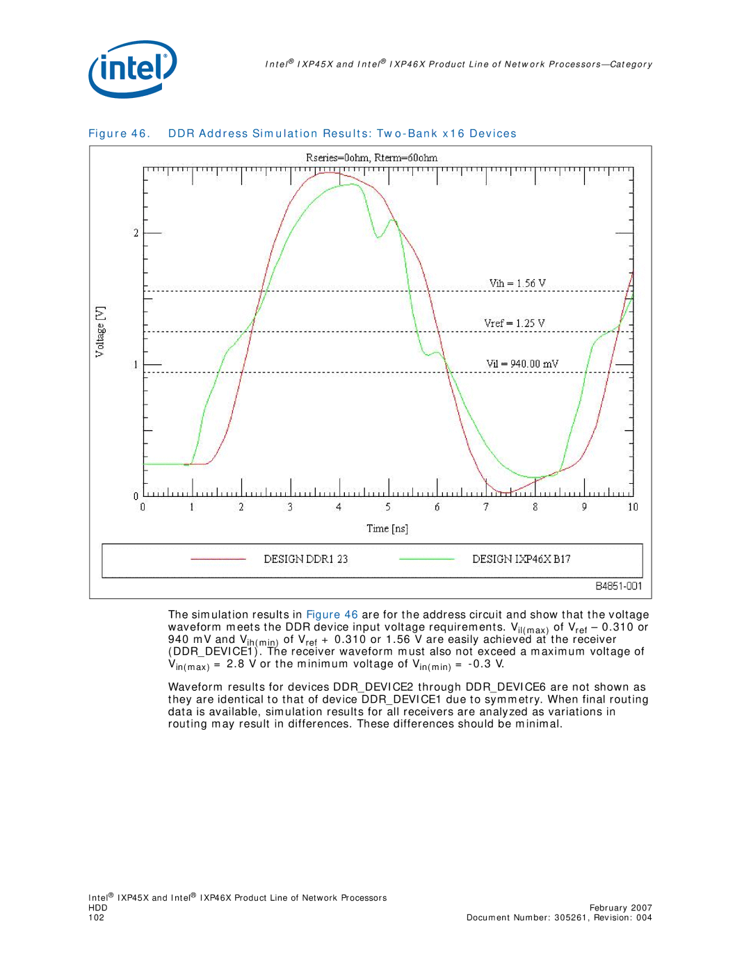
DDR Address Simulation Results Two-Bank x16 Devices
DDR Command RAS Topology Two-Bank x16 Devices
104
Rcvenin and Rcvenout
DDR RCVENIN/RCVENOUT Topology
DDR RCVENIN/RCVENOUT Simulation Results Rseries = 0 Ω
DDR RCVENIN/RCVENOUT Simulation Results Rseries = 60 Ω
108