7.0DDR-SDRAM
7.1Introduction
This document is intended to be used as a guide for routing DDR, based on the Intel® IXDP465 Development Platform. It contains routing guidelines and simulation results for using x16 Thin Small Outline Package (TSOP) memory devices soldered onto the processor module.
As shown in Figure 28, the Intel® IXP45X and Intel® IXP46X Product Line of Network Processors support two banks of
In this document, the term IXP45X/IXP46X product line refers to both the IXP46X network processors (with DDR ECC) and IXP45X network processors (without DDR ECC).
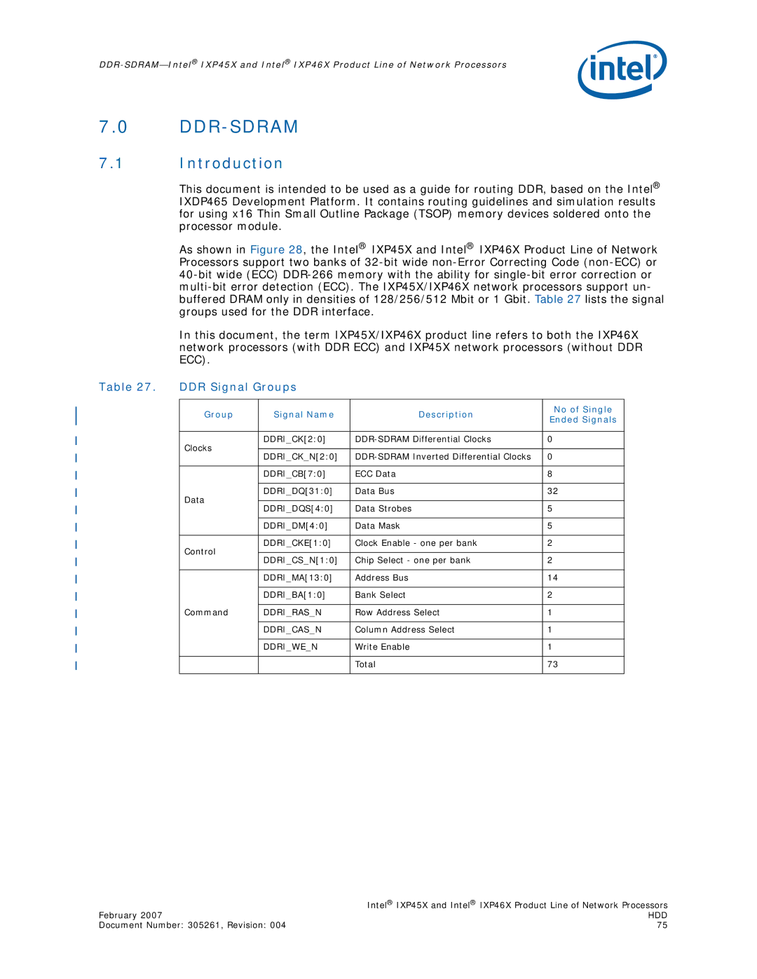
Table 27. | DDR Signal Groups |
|
| |
|
|
|
|
|
| Group | Signal Name | Description | No of Single |
| Ended Signals | |||
|
|
|
| |
|
|
|
|
|
| Clocks | DDRI_CK[2:0] | 0 | |
|
|
|
| |
| DDRI_CK_N[2:0] | 0 | ||
|
| |||
|
|
|
|
|
|
| DDRI_CB[7:0] | ECC Data | 8 |
|
|
|
|
|
| Data | DDRI_DQ[31:0] | Data Bus | 32 |
|
|
|
| |
| DDRI_DQS[4:0] | Data Strobes | 5 | |
|
| |||
|
|
|
|
|
|
| DDRI_DM[4:0] | Data Mask | 5 |
|
|
|
|
|
| Control | DDRI_CKE[1:0] | Clock Enable - one per bank | 2 |
|
|
|
| |
| DDRI_CS_N[1:0] | Chip Select - one per bank | 2 | |
|
| |||
|
|
|
|
|
|
| DDRI_MA[13:0] | Address Bus | 14 |
|
|
|
|
|
|
| DDRI_BA[1:0] | Bank Select | 2 |
|
|
|
|
|
| Command | DDRI_RAS_N | Row Address Select | 1 |
|
|
|
|
|
|
| DDRI_CAS_N | Column Address Select | 1 |
|
|
|
|
|
|
| DDRI_WE_N | Write Enable | 1 |
|
|
|
|
|
|
|
| Total | 73 |
|
|
|
|
|
| Intel® IXP45X and Intel® IXP46X Product Line of Network Processors |
February 2007 | HDD |
Document Number: 305261, Revision: 004 | 75 |
