Intel® IXP45X and Intel® IXP46X Product Line of Network
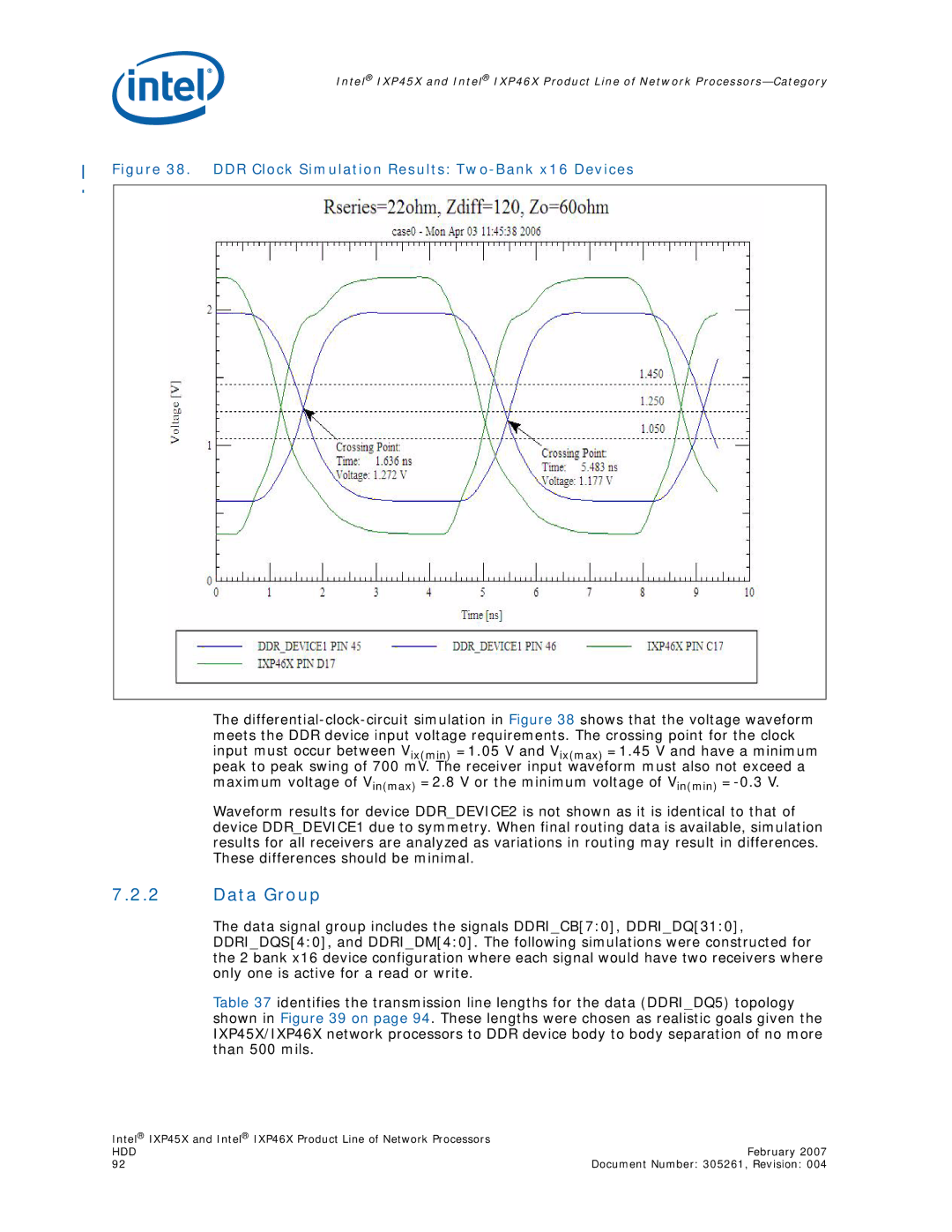
Figure 38. DDR Clock Simulation Results: Two-Bank x16 Devices
The
Waveform results for device DDR_DEVICE2 is not shown as it is identical to that of device DDR_DEVICE1 due to symmetry. When final routing data is available, simulation results for all receivers are analyzed as variations in routing may result in differences. These differences should be minimal.
7.2.2Data Group
The data signal group includes the signals DDRI_CB[7:0], DDRI_DQ[31:0],
DDRI_DQS[4:0], and DDRI_DM[4:0]. The following simulations were constructed for the 2 bank x16 device configuration where each signal would have two receivers where only one is active for a read or write.
Table 37 identifies the transmission line lengths for the data (DDRI_DQ5) topology shown in Figure 39 on page 94. These lengths were chosen as realistic goals given the IXP45X/IXP46X network processors to DDR device body to body separation of no more than 500 mils.
Intel® IXP45X and Intel® IXP46X Product Line of Network Processors |
|
HDD | February 2007 |
92 | Document Number: 305261, Revision: 004 |