Intel® IXP45X and Intel® IXP46X Product Line of Network
7.2Simulation Results
This section contains the simulation results for each of the DDR signal groups. Each of the signal groups may have different overall topologies based on the number of banks and ECC usage.
Each signal group simulated below uses a
7.2.1Clock Group
The clock signal group includes the differential clock pairs DDRI_CK[2:0] and
DDRI_CK_N[2:0]. The following simulation was constructed for the 2 bank x16 device configuration where each clock would have two receivers.
Table 36 identifies the transmission line lengths for the clock topology shown in Figure 37 on page 91. These lengths were chosen as realistic goals given the IXP45X/ IXP46X network processors to DDR device body to body separation of no more than 500 mils.
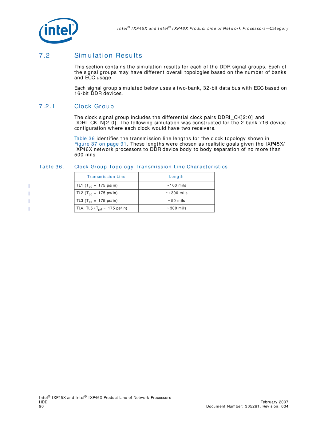
Table 36. Clock Group Topology Transmission Line Characteristics
Transmission Line | Length |
|
|
TL1 (Tpd = 175 ps/in) | ~100 mils |
TL2 (Tpd = 175 ps/in) | ~1300 mils |
TL3 (Tpd = 175 ps/in) | ~50 mils |
TL4, TL5 (Tpd = 175 ps/in) | ~300 mils |
Intel® IXP45X and Intel® IXP46X Product Line of Network Processors |
|
HDD | February 2007 |
90 | Document Number: 305261, Revision: 004 |