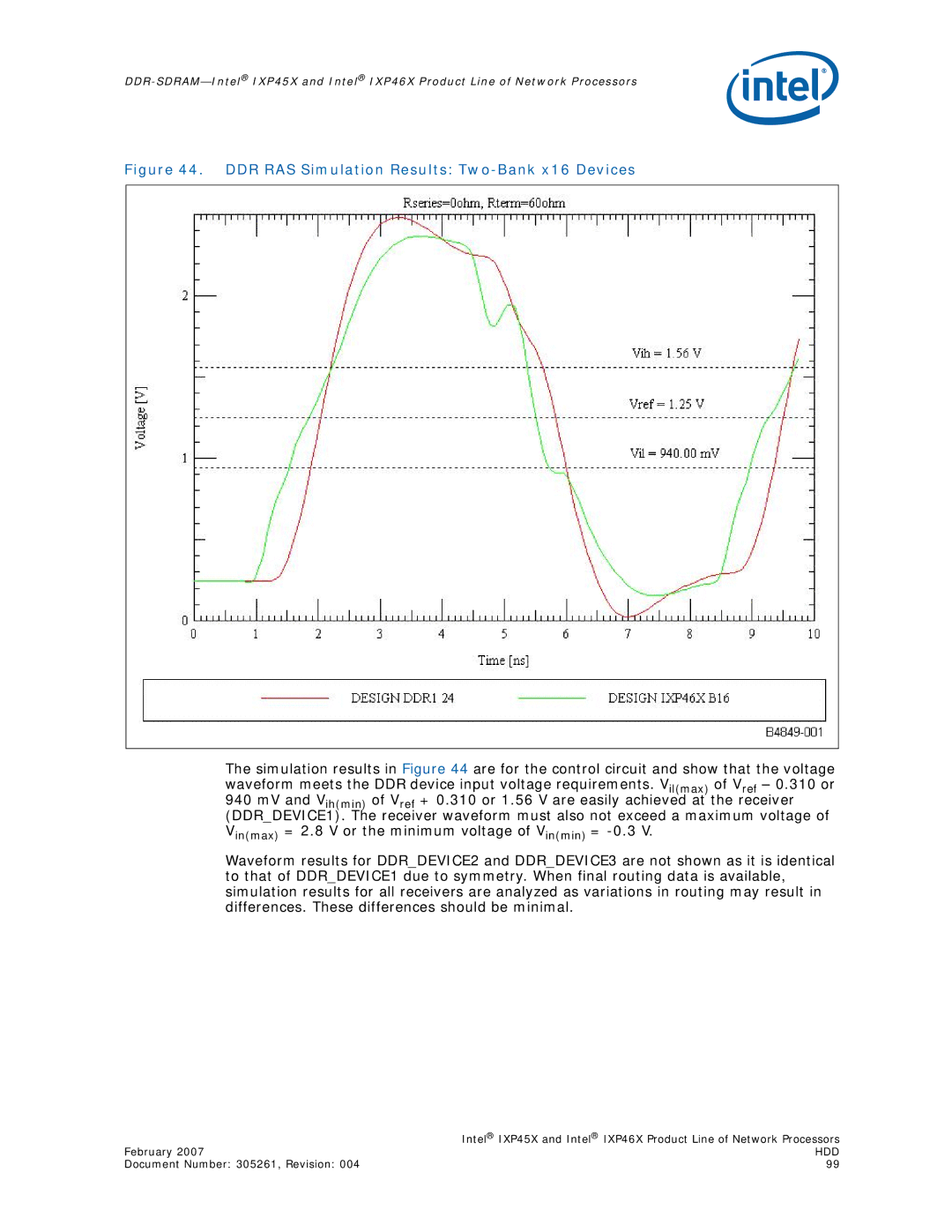
Figure 44. DDR RAS Simulation Results: Two-Bank x16 Devices
The simulation results in Figure 44 are for the control circuit and show that the voltage waveform meets the DDR device input voltage requirements. Vil(max) of Vref – 0.310 or 940 mV and Vih(min) of Vref + 0.310 or 1.56 V are easily achieved at the receiver (DDR_DEVICE1). The receiver waveform must also not exceed a maximum voltage of Vin(max) = 2.8 V or the minimum voltage of Vin(min) =
Waveform results for DDR_DEVICE2 and DDR_DEVICE3 are not shown as it is identical to that of DDR_DEVICE1 due to symmetry. When final routing data is available, simulation results for all receivers are analyzed as variations in routing may result in differences. These differences should be minimal.
| Intel® IXP45X and Intel® IXP46X Product Line of Network Processors |
February 2007 | HDD |
Document Number: 305261, Revision: 004 | 99 |