General Hardware Design
3.11.1Signal Interface
Table 19. | Synchronous Serial Peripheral Port Interface | |||
|
|
|
| |
| Input/ | Pull |
| |
Name | Up/ | Recommendations | ||
Output | ||||
| Down |
| ||
|
|
|
| |
SSP_SCLK | O | No | Serial bit clock. | |
|
|
|
| |
SSP_SFRM | O | No | Serial frame indicator. | |
|
|
|
| |
SSP_TXD | O | No | Transmit data (serial data out). | |
|
|
|
| |
SSP_RXD | I | Yes | Receive data (serial data in). | |
Should be pulled high through a | ||||
|
|
| ||
|
|
|
| |
SSP_EXTCLK | I | Yes | External clock input. | |
Should be pulled high through a | ||||
|
|
| ||
|
|
|
| |
3.11.2Device Connection
There are a number of devices available that can interface to SSP or SPI ports, these can range from RTC
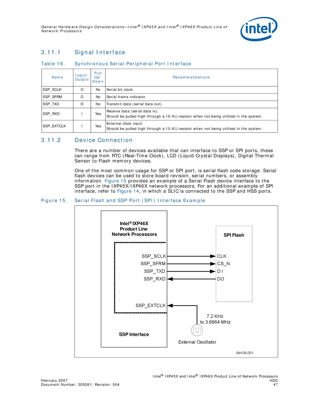
One of the most common usage for SSP or SPI port, is serial flash code storage. Serial flash devices can be used to store board revision, serial numbers, or assembly information. Figure 15 provides an example of a Serial Flash device interface to the SSP port in the IXP45X/IXP46X network processors. For an additional example of SPI interface, refer to Figure 14, in which a SLIC is connected to the SSP and HSS ports.
Figure 15. Serial Flash and SSP Port (SPI) Interface Example
Intel® IXP46X |
| |||||
Product Line |
| |||||
Network Processors | SPI Flash | |||||
SSP_SCLK |
|
|
| CLK | ||
|
| |||||
SSP_SFRM |
|
|
| CS_N | ||
|
| |||||
SSP_TXD |
|
|
|
|
| D I |
|
|
| ||||
SSP_RXD |
| DO | ||||
| ||||||
|
|
|
|
|
|
|
SSP_EXTCLK ![]()
7.2 KHz to 3.6864 MHz
SSP Interface
External Oscillator
| Intel® IXP45X and Intel® IXP46X Product Line of Network Processors |
February 2007 | HDD |
Document Number: 305261; Revision: 004 | 47 |