Hardware Design Guidelines
February
Document No 305261 Revision
February
Introduction
Contents
Document Number 305261, Revision
February
5.0 General Layout and Routing Guide
6.0 PCI Interface Design Considerations
Figures
Tables
Description
Revision History
Date
Revision
February
1.0Introduction
1.1Content Overview
1.2Related Documentation
1.3Acronyms and Abbreviations
1.4Overview
List of Acronyms and Abbreviations
32-bitPCI interface Master/Target 33/66 MHz
Unit
Figure 1. Intel IXP465 Component Block Diagram
MII/SMII
Cryptography
1.5Typical Applications
2.0System Architecture
2.1System Architecture Description
2.2System Memory Map
Processors
JTAG
IntelIXP46X Product
Line of Network
Table
3.1Soft Fusible Features
Signal Type Definitions
3.0General Hardware Design Considerations
DDR SDRAM Interface Pin Description Sheet 1 of
3.2.1Signal Interface
Soft Fusible Features
3.2DDR-266SDRAM Interface
DDR SDRAM Interface Pin Description Sheet 2 of
3.3Expansion Bus
3.2.2DDR SDRAM Memory Interface
3.2.3DDR SDRAM Initialization
3.3.1Signal Interface
3.3.2Reset Configuration Straps
Expansion Bus Signal Recommendations
Function
Boot/Reset Strapping Configuration Sheet 1 of
Table
Name
Boot/Reset Strapping Configuration Sheet 2 of
3.3.38-BitDevice Interface
3.3.416-BitDevice Interface
3.3.532-BitDevice Interface
8-BitDevice
Byte Access
16-Bit-WordAccess
32-Bit-WordAccess
8-BitDevice
Byte Access
16-Bit-WordAccess
32-Bit-WordAccess
16-Bit-WordAccess
Intel Flash
3.3.6Flash Interface
Figure 5. Flash Interface Example
Figure 6. Expansion Bus SRAM Interface
3.4UART Interface
3.3.7SRAM Interface
3.3.8Design Notes
UART Signal Recommendations
3.4.1Signal Interface
UART Interface
Connector
MII/SMII Interface
Figure 7. UART Interface Example
3.5.1Signal Interface MII
MII NPE A Signal Recommendations
MII NPE B Signal Recommendations Sheet 1 of
MII NPE C Signal Recommendations
MII NPE B Signal Recommendations Sheet 2 of
3.5.2Device Connection, MII
Figure 8. MII Interface Example
10/100
3.5.3Signal Interface, SMII
3.6GPIO Interface
3.5.4Device Connection, SMII
Figure 9. SMII Interface Example
3.6.1Signal Interface
GPIO Signal Recommendations
3.6.2Design Notes
3.7.2Device Connection
3.7.1Signal Interface
I2C Signal Recommendations
3.7I2C Interface
Network Processor
3.8USB Interface
Figure 10. I2C EEPROM Interface Example
Product Line
USB Host/Device Signal Recommendations
3.8.1Signal Interface
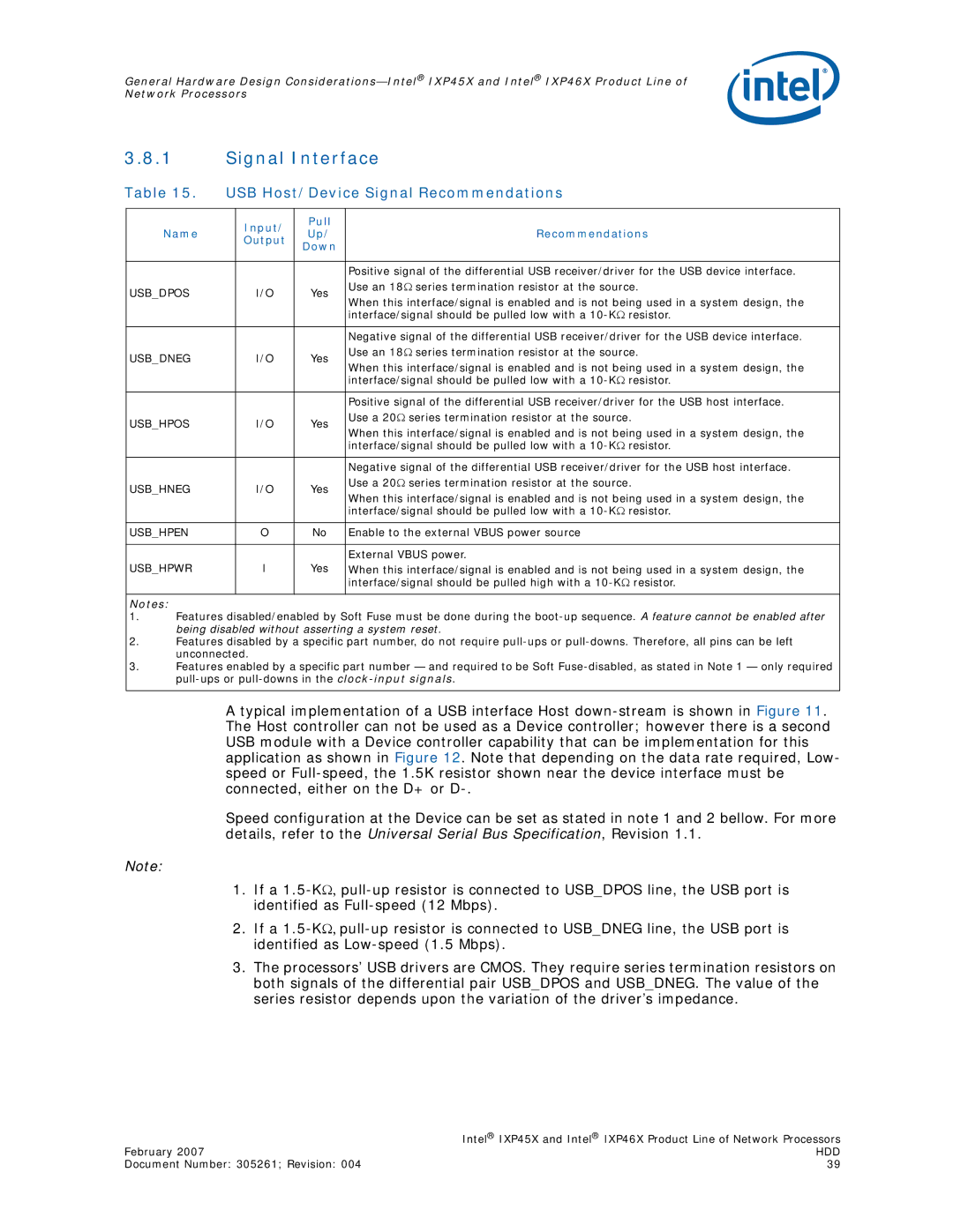
Device
3.8.2Device Connection
Figure 11. USB Host Down Stream Interface Example
Host
Host
3.9UTOPIA Level 2 Interface
Figure 12. USB Device Interface Example
Device
3.9.1Signal Interface
UTOPIA Signal Recommendations
3.9.2Device Connection
ATM Layer Device
3.10HSS Interface
Figure 13. UTOPIA Interface Example
Analog Front
High-Speed,Serial Interface
3.10.1Signal Interface
Transmit frame
High-Speed,Serial Interface
3.11SSP Interface
3.10.2Device Connection
Figure 14. HSS Interface Example
SPI Flash
3.11.1Signal Interface
3.11.2Device Connection
Synchronous Serial Peripheral Port Interface
3.12.1Signal Interface
3.12PCI Interface
PCI Controller Sheet 1 of
PCI Controller Sheet 2 of
3.12.2PCI Interface Block Diagram
cPCI J1
3.12.3Supporting 5 V PCI Interface
Figure 16. PCI Interface
Compact PCI Bus
PCI Device
3.12.4PCI Option Interface
3.3V Logic
PCI Device
Page
3.12.5Design Notes
3.13JTAG Interface
3.14Input System Clock
3.13.1Signal Interface
3.14.1Clock Signals
Clock Signals
3.15Power
3.14.3Device Connection
Intel IXP46X
3.15.1De-CouplingCapacitance Recommendations
3.15.5Power Sequence
3.15.6Reset Timing
Power Interface Sheet 2 of
Document Number 305261 Revision
February
Document Number 305261 Revision
February
4.2General Recommendations
4.4Component Placement
4.0General PCB Guide
4.1PCB Overview
Medium Frequency
Figure 19. Component Placement on a PCB
4.5Stack-UpSelection
Inexpensive
Poor routing density
Uncontrolled signal trace impedance
Low-impedancepower distribution
Higher cost More weight
Figure 21. 6-LayerStackup
Figure 20. 8-LayerStackup
5.0General Layout and Routing Guide
5.1Overview
5.2General Layout Guidelines
Figure 22. Signal Changing Reference Planes
5.2.1General Component Spacing
VIAs
Figure 24. Poor Design Practice for VIA Placement
25 mils min 25 mils min 25 mils min
Flush Via min Potential Bridge min
PGA or BGA Package
5.2.2Clock Signal Considerations
5.2.3SMII Signal Considerations
5.2.4MII Signal Considerations
5.2.5USB Considerations
5.2.7EMI-DesignConsiderations
5.2.6Cross-Talk
Document Number 305261 Revision
5.2.9Power and Ground Plane
5.2.8Trace Impedance
February
Document Number 305261 Revision
February
6.0PCI Interface Design Considerations
6.1Electrical Interface
6.2Topology
Table 25. PCI Address/Data Routing Guidelines
6.3Clock Distribution
Figure 26. PCI Address/Data Topology
PCI Slot
Driver
6.3.1Trace Length Limits
PCI Devices
Clock
6.3.3Signal Loading
6.3.2Routing Guidelines
February
Table
DDR Signal Groups
7.0DDR-SDRAM
7.1Introduction
DDR SDRAM
Figure 28. Processor-DDRInterface
Processors
Line of Network
Document Number: 305261, Revision:
February
Supported Memory Configurations
Intel IXP46X
VTT Signal Termination
Signal
Termination
DDR SDRAM
7.1.1Selecting VTT Power Supply
Figure 30. VTT Terminating Circuitry
IXP46X
7.1.2Signal-TimingAnalysis
Figure 31. DDR Command and Control Setup and Hold
Control/Command Valid
DDR M CLK
Figure 32. DDR Data to DQS Read Timing Parameters
Data
DDR Data to DQS Read Timing Parameters
Data
Figure 33. DDR-Data-to-DQS-WriteTiming Parameters
Data Valid
DDR Data to DQS Write Timing Parameters
DDR-Clock-to-DQS-WriteTiming Parameters
7.1.3Printed Circuit Board Layer Stackup
Figure 35. Printed Circuit Board Layer Stackup
7.1.4Printed Circuit Board Controlled Impedance
February
Figure 32 on page -Table 30 on page
7.1.5Timing Relationships
Figure 31 on page -Table 29 on page
—Table 30 on page —Table 31 on page
7.1.6Resistive Compensation Register Rcomp
7.1.7Routing Guidelines
7.1.7.1Clock Group
Clock Signal Group Routing Guidelines
7.1.7.2Data, Command, and Control Groups
7.2.1Clock Group
7.2Simulation Results
Document Number: 305261, Revision:
February
February
7.2.2Data Group
TL1 Tpd = 175 ps/in
February
Figure 39. DDR Data Topology Two-Bankx16 Devices
Document Number: 305261, Revision:
February
February
Document Number 305261, Revision
February
7.2.3Control Group
Document Number 305261, Revision
February
TL3 Tpd = 175 ps/in
7.2.4Command Group
TL1 Tpd = 175 ps/in
TL2 Tpd = 175 ps/in
Document Number 305261, Revision
February
February
Document Number 305261, Revision
February
February
Figure 49. DDR RCVENIN/RCVENOUT Topology
7.2.5RCVENIN and RCVENOUT
February
Document Number 305261, Revision
February
Document Number 305261, Revision
February