Philips Semiconductors | User’s Manual - Preliminary - | |
|
|
|
I/O PORTS | P89LPC906/907/908 |
|
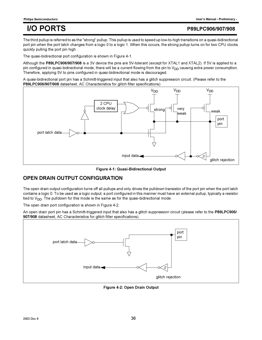
The third pullup is referred to as the "strong" pullup. This pullup is used to speed up
The
Although the P89LPC906/907/908 is a 3V device the pins are
A
VDD | VDD | VDD |
port latch data

|
|
|
|
|
|
|
|
|
|
|
|
|
|
|
|
|
|
|
|
|
|
|
|
|
|
|
|
|
| 2 CPU |
|
|
|
|
|
|
|
|
|
|
|
|
|
|
|
|
|
|
|
|
|
|
|
|
|
|
|
|
|
|
|
|
|
|
|
|
|
|
|
|
|
|
|
|
|
|
|
|
|
|
|
|
|
|
| |
| clock delay |
|
|
|
|
|
|
|
|
| strong |
|
|
|
|
| very |
|
|
|
|
| weak | |||||
|
|
|
|
|
|
|
|
|
|
|
|
|
|
| ||||||||||||||
|
|
|
|
|
|
|
|
|
|
|
|
|
|
|
|
|
|
|
| |||||||||
|
|
|
|
|
|
|
|
|
|
|
|
|
|
|
|
|
|
| weak |
|
|
| ||||||
|
|
|
|
|
|
|
|
|
|
|
|
|
|
|
|
|
|
|
|
|
|
|
|
| ||||
|
|
|
|
|
|
|
|
|
|
|
|
|
|
|
|
|
|
|
|
|
|
|
|
|
|
|
| port |
|
|
|
|
|
|
|
|
|
|
|
|
|
|
|
|
|
|
|
|
|
|
|
|
|
|
|
| pin |
|
|
|
|
|
|
|
|
|
|
|
|
|
|
|
|
|
|
|
|
|
|
|
|
|
|
|
|
|
|
|
|
|
|
|
|
|
|
|
|
|
|
|
|
|
|
|
|
|
|
|
|
|
|
|
|
|
|
|
|
|
|
|
|
|
|
|
|
|
|
|
|
|
|
|
|
|
|
|
|
|
|
|
|
|
|
|
|
|
|
|
|
|
|
|
|
|
|
|
|
|
|
|
|
|
|
|
|
|
|
|
|
|
|
|
|
|
|
|
|
|
|
|
|
|
|
|
|
|
|
|
|
|
|
|
|
|
|
|
|
|
|
|
|
|
input data ![]()
glitch rejection
Figure 4-1: Quasi-Bidirectional Output
OPEN DRAIN OUTPUT CONFIGURATION
The open drain output configuration turns off all pullups and only drives the pulldown transistor of the port pin when the port latch contains a logic 0. To be used as a logic output, a port configured in this manner must have an external pullup, typically a resistor tied to VDD. The pulldown for this mode is the same as for the
The open drain port configuration is shown in Figure
An open drain port pin has a
port latch data![]()
![]()
![]()
![]()
input data![]()
port |
pin |
glitch rejection
Figure 4-2: Open Drain Output
2003 Dec 8 | 36 |