Philips Semiconductors | User’s Manual - Preliminary - | |
|
|
|
I/O PORTS | P89LPC906/907/908 | |
|
|
|
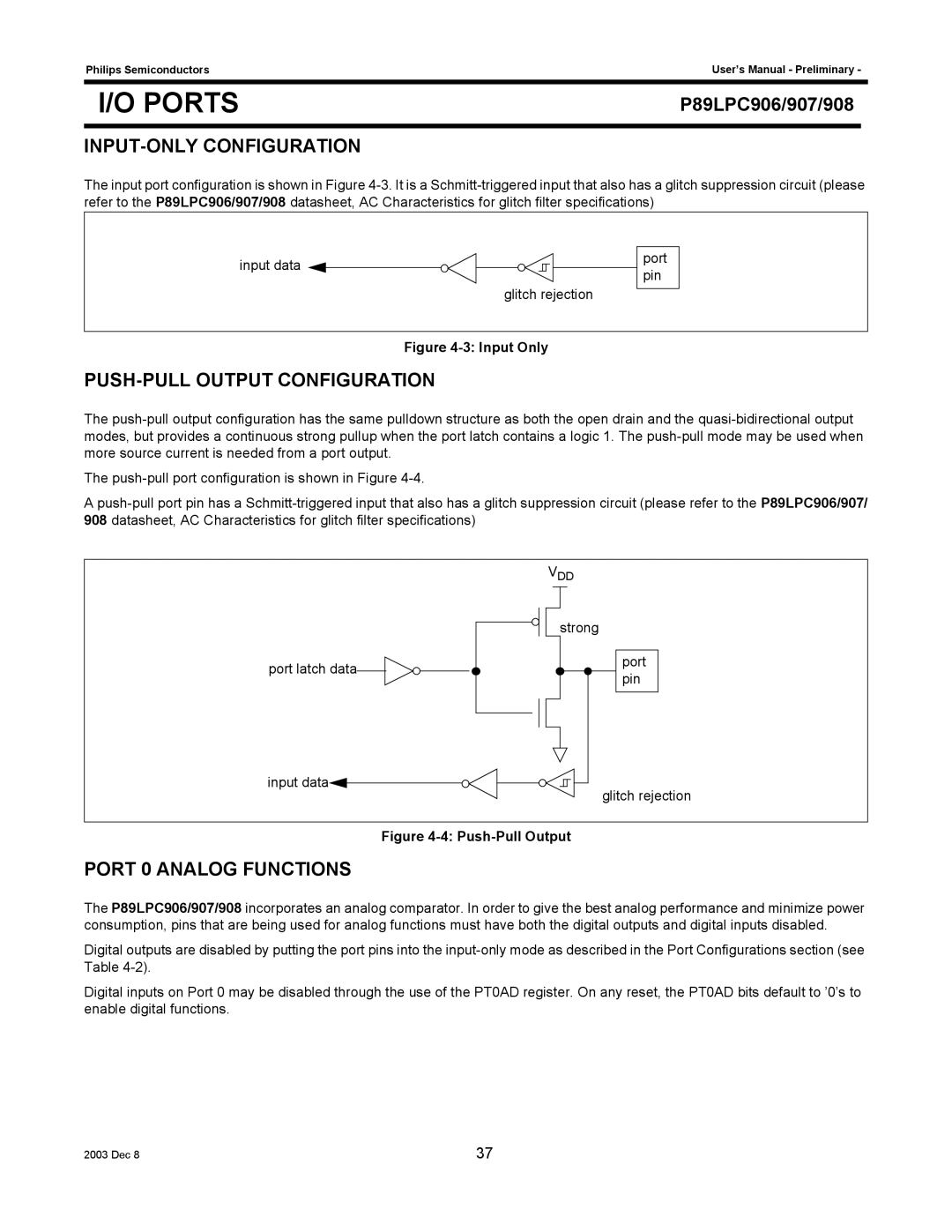
The input port configuration is shown in Figure
input data ![]()
glitch rejection
port pin
Figure 4-3: Input Only
PUSH-PULL OUTPUT CONFIGURATION
The
The
A
VDD
strong
port latch data


port pin
input data 
glitch rejection
Figure 4-4: Push-Pull Output
PORT 0 ANALOG FUNCTIONS
The P89LPC906/907/908 incorporates an analog comparator. In order to give the best analog performance and minimize power consumption, pins that are being used for analog functions must have both the digital outputs and digital inputs disabled.
Digital outputs are disabled by putting the port pins into the
Digital inputs on Port 0 may be disabled through the use of the PT0AD register. On any reset, the PT0AD bits default to ’0’s to enable digital functions.
2003 Dec 8 | 37 |
