Philips Semiconductors |
|
|
|
|
| User’s Manual - Preliminary - | |||||
|
|
|
|
|
|
|
|
|
|
|
|
I/O PORTS |
|
|
|
| P89LPC906/907/908 | ||||||
Table |
|
|
|
|
| ||||||
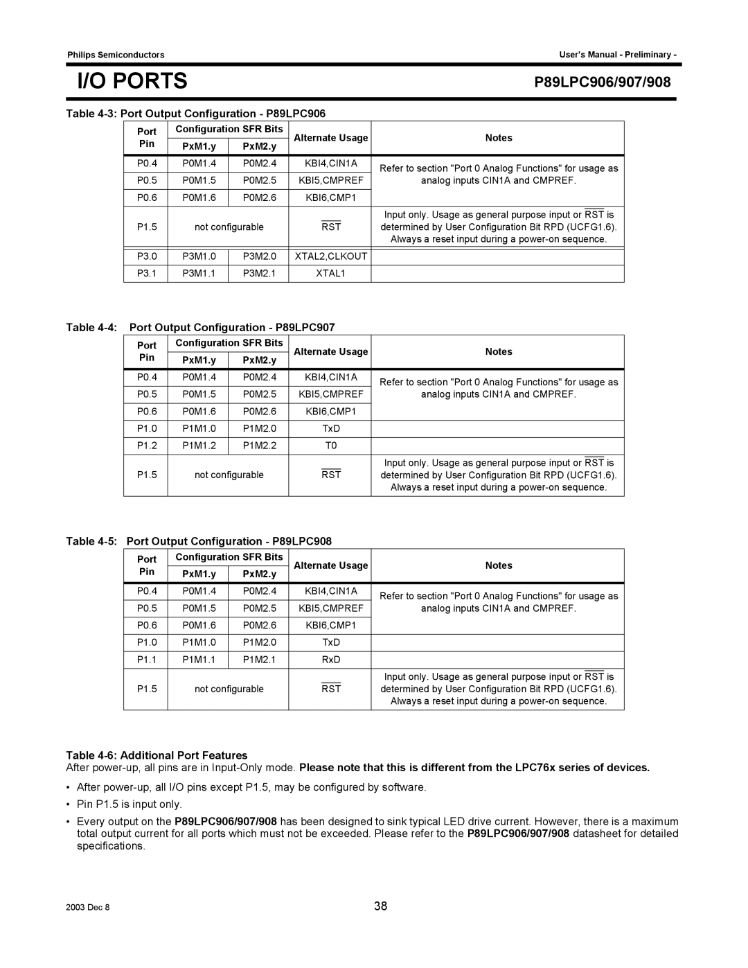
| Port | Configuration SFR Bits | Alternate Usage | Notes |
|
| |||||
| Pin | PxM1.y | PxM2.y |
|
| ||||||
|
|
|
|
|
|
|
|
| |||
| P0.4 | P0M1.4 | P0M2.4 | KBI4,CIN1A | Refer to section "Port 0 Analog Functions" for usage as |
|
| ||||
|
|
|
|
|
|
|
| ||||
| P0.5 | P0M1.5 | P0M2.5 | KBI5,CMPREF | analog inputs CIN1A and CMPREF. |
|
| ||||
|
|
|
|
|
|
|
|
|
| ||
| P0.6 | P0M1.6 | P0M2.6 | KBI6,CMP1 |
|
|
|
|
| ||
|
|
|
|
|
|
|
|
|
|
| |
|
|
|
|
|
|
| Input only. Usage as general purpose input or |
| is |
| |
|
|
|
|
|
|
| RST | ||||
| P1.5 | not configurable |
| RST |
| determined by User Configuration Bit RPD (UCFG1.6). |
| ||||
|
|
|
|
|
|
| Always a reset input during a |
| |||
|
|
|
|
|
|
|
|
|
|
|
|
| P3.0 | P3M1.0 | P3M2.0 | XTAL2,CLKOUT |
|
|
|
|
| ||
|
|
|
|
|
|
|
|
|
| ||
| P3.1 | P3M1.1 | P3M2.1 | XTAL1 |
|
|
|
|
| ||
|
|
|
|
|
|
|
|
|
| ||
Table |
|
|
|
|
| ||||||
| Port | Configuration SFR Bits | Alternate Usage | Notes |
|
| |||||
| Pin | PxM1.y | PxM2.y |
|
| ||||||
|
|
|
|
|
|
|
|
| |||
| P0.4 | P0M1.4 | P0M2.4 | KBI4,CIN1A | Refer to section "Port 0 Analog Functions" for usage as |
|
| ||||
|
|
|
|
|
|
|
| ||||
| P0.5 | P0M1.5 | P0M2.5 | KBI5,CMPREF | analog inputs CIN1A and CMPREF. |
|
| ||||
|
|
|
|
|
|
|
|
|
| ||
| P0.6 | P0M1.6 | P0M2.6 | KBI6,CMP1 |
|
|
|
|
| ||
|
|
|
|
|
|
|
|
|
|
| |
| P1.0 | P1M1.0 | P1M2.0 |
| TxD |
|
|
|
|
| |
|
|
|
|
|
|
|
|
|
|
| |
| P1.2 | P1M1.2 | P1M2.2 |
| T0 |
|
|
|
|
| |
|
|
|
|
|
|
|
|
|
|
| |
|
|
|
|
|
|
| Input only. Usage as general purpose input or |
| is |
| |
| P1.5 | not configurable |
|
|
| RST | |||||
|
| RST |
| determined by User Configuration Bit RPD (UCFG1.6). |
| ||||||
|
|
|
|
|
|
| Always a reset input during a |
| |||
|
|
|
|
|
|
|
|
| |||
Table |
|
|
|
|
| ||||||
| Port | Configuration SFR Bits | Alternate Usage | Notes |
|
| |||||
| Pin | PxM1.y | PxM2.y |
|
| ||||||
|
|
|
|
|
|
|
|
| |||
| P0.4 | P0M1.4 | P0M2.4 | KBI4,CIN1A | Refer to section "Port 0 Analog Functions" for usage as |
|
| ||||
|
|
|
|
|
|
|
| ||||
| P0.5 | P0M1.5 | P0M2.5 | KBI5,CMPREF | analog inputs CIN1A and CMPREF. |
|
| ||||
|
|
|
|
|
|
|
|
|
| ||
| P0.6 | P0M1.6 | P0M2.6 | KBI6,CMP1 |
|
|
|
|
| ||
|
|
|
|
|
|
|
|
|
|
| |
| P1.0 | P1M1.0 | P1M2.0 |
| TxD |
|
|
|
|
| |
|
|
|
|
|
|
|
|
|
|
| |
| P1.1 | P1M1.1 | P1M2.1 |
| RxD |
|
|
|
|
| |
|
|
|
|
|
|
|
|
|
|
| |
|
|
|
|
|
|
| Input only. Usage as general purpose input or |
| is |
| |
| P1.5 | not configurable |
|
|
| RST | |||||
|
| RST |
| determined by User Configuration Bit RPD (UCFG1.6). |
| ||||||
|
|
|
|
|
|
| Always a reset input during a |
| |||
|
|
|
|
|
|
|
|
|
|
|
|
Table
After
•After
•Pin P1.5 is input only.
•Every output on the P89LPC906/907/908 has been designed to sink typical LED drive current. However, there is a maximum total output current for all ports which must not be exceeded. Please refer to the P89LPC906/907/908 datasheet for detailed specifications.
2003 Dec 8 | 38 |