Philips Semiconductors |
|
| User’s Manual - Preliminary - | ||
|
|
|
|
|
|
FLASH PROGRAM MEMORY | P89LPC906/907/908 | ||||
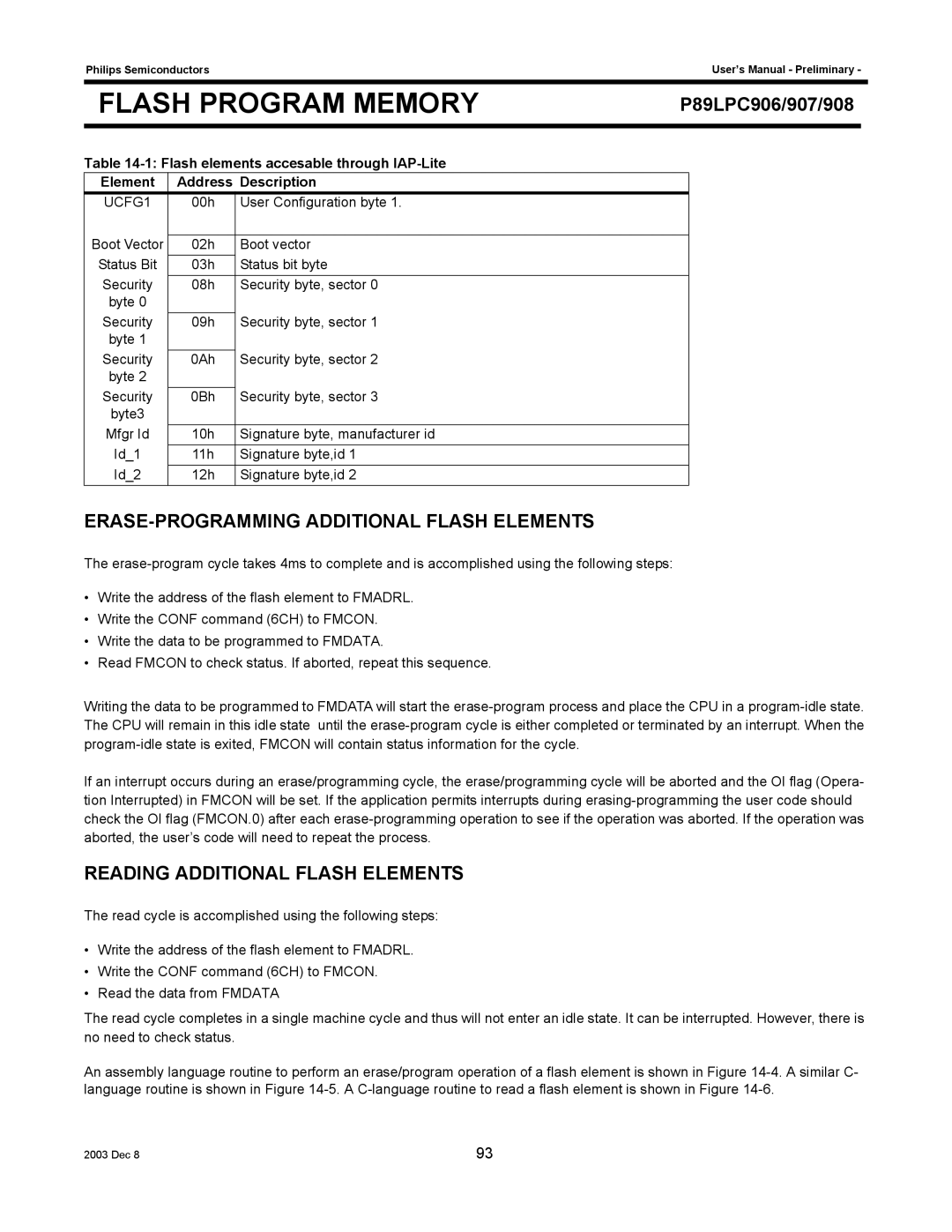
Table |
|
|
| ||
Element | Address Description |
|
|
| |
UCFG1 | 00h | User Configuration byte 1. |
|
|
|
Boot Vector |
|
|
|
|
|
02h | Boot vector |
|
|
| |
Status Bit | 03h | Status bit byte |
|
|
|
Security | 08h | Security byte, sector 0 |
|
|
|
byte 0 |
|
|
|
|
|
Security | 09h | Security byte, sector 1 |
|
|
|
byte 1 |
|
|
|
|
|
Security | 0Ah | Security byte, sector 2 |
|
|
|
byte 2 |
|
|
|
|
|
Security | 0Bh | Security byte, sector 3 |
|
|
|
byte3 |
|
|
|
|
|
Mfgr Id | 10h | Signature byte, manufacturer id |
|
|
|
Id_1 | 11h | Signature byte,id 1 |
|
|
|
Id_2 | 12h | Signature byte,id 2 |
|
|
|
ERASE-PROGRAMMING ADDITIONAL FLASH ELEMENTS
The
•Write the address of the flash element to FMADRL.
•Write the CONF command (6CH) to FMCON.
•Write the data to be programmed to FMDATA.
•Read FMCON to check status. If aborted, repeat this sequence.
Writing the data to be programmed to FMDATA will start the
If an interrupt occurs during an erase/programming cycle, the erase/programming cycle will be aborted and the OI flag (Opera- tion Interrupted) in FMCON will be set. If the application permits interrupts during
READING ADDITIONAL FLASH ELEMENTS
The read cycle is accomplished using the following steps:
•Write the address of the flash element to FMADRL.
•Write the CONF command (6CH) to FMCON.
•Read the data from FMDATA
The read cycle completes in a single machine cycle and thus will not enter an idle state. It can be interrupted. However, there is no need to check status.
An assembly language routine to perform an erase/program operation of a flash element is shown in Figure
2003 Dec 8 | 93 |